John's FPGA Page
Resources and projects for FPGA design.
http://members.optusnet.com.au/jekent/FPGA.htm
Page Last Updated 09/03/2012 10:39 PM
Contents:
1. VHDL - References and Tutorials:2. FPGA Manufacturers & Board Vendors:3. FPGA Prototyping Boards I Use:3.1 BurchED B3-Spartan2+ Board4. FPGA Design Tools:3.1.1 ICST525-01 PLL Clock divider3.2 BurchED B5-X300-Spartan2e Board
3.1.2 Notes on modifying the B3-SRAM module
3.1.3 Notes on adding a CF card
3.3 Digilent Spartan 3 Starter Board
3.4 Digilent Spartan 3E Starter Board
3.5 XESS XSA-3S1000, XST-3.0 & XSUSB3.5.1 IDE Compact Flash Interface.3.6 Memec Design / Avnet V4FX12LC
3.7 Altera / Terasic DE2-70 Cyclone 2
3.8 Altera / Terasic DE1 Cyclone 2
3.9 XESS XuLA Spartan 3A4.1 Xilinx Web Pack ISE:5. FPGA Projects
4.2 Altera Quartus:5.1 System16 - My Initial VHDL CPU Project6. VHDL & Verilog IP Resource Links:
5.2 Memio.zip Memory I/O Tool
5.3 Micro8 - A very simple microprocessor
5.4 Micro8a - Adding a Stack
5.5 Micro16 - Very Basic 16 bit machine
5.6 Micro16 - Processing Array
5.7 Motorola 8 bit CPUs
5.8 System01 - 6801 - Working (Incomplete I/O)
5.9 System68 - 6800 - Working
5.10 System05 - 6805 - Work in Progress
5.11 System11 - 68HC11 - Partly Working
5.12 System09 - 6809 SOC - Runs Flex9 with VDU and PS/2 Keyboard
5.13 System6801 - Wishbone Compliant 6801 for Altera by Michael Hasenfratz
1. VHDL - References and Tutorials:
The two most common languages used for FPGA design are VHDL and Verilog. I have chosen to use VHDL for my designs for no other reason than the reference books appeared to be a bit cheaper and more readily available. VHDL stands for Very high speed integrated circuit Hardware Description Language
Here are some of the VHDL online Tutorials thrown up by Google:VHDL-online - by Prof. Dr.-Ing. Wolfram H. Glauert, Universität Erlangen-Nürnberg
VHDL Introductory Tutorial - Green Mountain Computing Systems Inc.
Tutorial: Learn by Example - by Weijun Zhang, University of California Riversdale
VHDL Tutorial - Jan Van der Spiegel, University of Pennsylvania
VHDL Cookbook (pdf) - by Peter J. Ashenden - Dept. Computer Science, University of Adelaide South Australia (Hosted by Hamburg University).
VHDL Verification Course - www.stefanvhdl.com
VHDL Handbook - HARDI Electronics (Hosted www.cs.umbc.edu)
FPGA Training Videos by Burch Electronic Design
My good friend Anthony Burch up in Sydney has developed a series of FPGA training videos especially designed for newcomers to FPGA design. They are suitable for hobbyists, university students, commercial organizations and engineers wishing to learn about FPGAs. Membership to the web site is only AU$19.95 and gives you access to 18 videos.Tony offers the first 6 videos free as an introduction to give you an idea of what to expect.
The topics include:
- What to look for in selecting an FPGA board
- Downloading and installing the Xilinx Web pack software,
- Designing a simple logic circuit for the Xilinx Spartan 3E starter board,
- Using schematic capture, and
- Downloading the code to the FPGA board.
Tony has had many years of experience in developing FPGA systems, having designed the B3-Spartan2+ and B5-X300 FPGA boards, and add on modules.
Tony's videos were featured in Max Maxfield's Programmable Logic Design Line newsletter on the 21st August 2008.
http://www.pldesignline.com/blogs/210101879
http://www.diycalculator.com/ - Clive (Max) Maxfield's and Alvin Brown's DIY Calculator web site
This is Max & Alvin's web site for their book "How Computers Do Maths" which describes a basic 8 bit microprocessor and the assembler routines for performing maths functions. Max & Alvin provide an emulator for their virtual 8 bit microprocessor CPU which can be downloaded from the web site. They have also produced a data book for their CPU chip along the lines of the assembly instructions manuals for the early 8 bit chips. The data data book is also available for download. The book provides an excellent introduction to basic micro-computing.
Heaps of books can also be found on Amazon, by using the key words "FPGA", "VHDL", Verilog", "Xilinx" and "Altera".
Amr Ali has a number of slides entitled VHDL 360 by his friends Mohamed Samy and Samer El-Saadany
Synthesis Examples
Synthesis Using ISE
Data Types and Operators
Data Types and Oporations Continued
Create Your First Model for a Simple Logic Circuit
Write More Complex Models
Write More Complex Models Continued
Modeling Finite State Machines(FSMs)
Structural Description
Post Place and Route Simulation
Simulation using ISIM
uCOS & VHDL Training
Amr, Samy and Samer also offer uCOS II & III on-line training, for embedded CPUs and online courses in VHDL for Xilinx FPGAs. They also give instructor lead courses for those who are interested. Courses are tools independent and are mainly based on simulations. Contact amraldo@hotmail.com for course details.
Electronic Forum for the Electrical Engineering Community. Covers Analog Design, RF Design, Power Management, Embedded Design, Test & Measure, Components & PCB Design. EEWeb have kindly offered to feature this web site on their home page on the 5th September 2011.
2. FPGA Manufactures & Board Vendors:
Here is a list of vendors of low price Xilinx (mostly Spartan) FPGA boards suitable for hobby use.Altera - FPGA Manufacturer (Cyclone, Arria, Statix)
Lattice - FPGA Manufacturer (XP, Mach, SC, EC, ECP)
Xilinx - FPGA Manufacturer (Spartan & Virtex)
Avnet (US)
A wide range of Spartan 3, Virtex 2, Virtex 2 Pro, Virtex 4 and Virtex 5 boards
Too many to list. More intended for professional use.
Braemac (Australia)
Australian Altera/Terasic Distributor
BurchED (Australia)
Xilinx FPGA Video Guides
(Formerly Spartan2 B3 (XC2S200), B5 & B5-X300 (XC2S300))
Digilent Inc (US)
XUP (Virtex 2)
NetFPGA (Virtex2 Pro)
GENESYS (Virtex5)
OPUS (Virtex 5)
BASYS2 (Spartan 3E XC3S100E, XC3S250E)
NEXSYS2 (Spartan 3E XC3S500E, XC3S1200E)
Spartan3 Starter Board (XC3S200, XC3S1000)
Spartan3E Starter Board (XC3S500E, XC3S1600E)Falulous Silicon
Gadget Factory
Alien Cortex Board Multicore softprocessor development platform by Bryan Pape.\
Butterfly One (XC3S250E is $49.99 and the XC3S500E $74.99)
Seed Studio (Gadget Factory supplier)
Papilio One (XC3S250E board is $49.90 and the XC3S500E $64.90) and there are other suppliers in US and UK.
KNJN LLC (US)
RS232: Pluto (ACEX-1K), Pluto-II (Cyclone EP1K10), Pluto-3 (Cyclone II EP2C5)
Parallel: Pluto-P (ACEX EP1K10)
USB2: Saxo (Cyclone EP1C3), Saxo-L (Cyclone EP1C3 - Optional ARM CPU), Saxo-Q (Cyclone EP2C5 - 4 input ADC)
USB2: Xylo (Cyclone EP1C3), Xylo-EM (Cyclone EP2C5), Xylo-L (Spartan3E XC3S500E - NXP ARM CPU)
PCI: Dragon (Spartan2 XC2S100 PCI)
PCI-E: Dragon-E (Virtex5 XC5VLX20T PCI-E)
Trenz Electronics (Germany)
TE0140 Series (Spartan 3) Standard FPGA Micromodules
TE0300 Series (Spartan 3E) Industrial FPGA Micromodules
TE0320 Series (Spartan-3A DSP) Industrial Micromodule Series
Xess (US)
XSA-3S1000 - (Spartan 3 XC3S1000)
XuLA - (Spartan 3A XC3S50A, XC3S200A)
XST-4.0 - Extender Board
XSUSB - USB Interfface
Dr Dave Vanden Bout runs a Yahoo mailing list to support his boards http://tech.groups.yahoo.com/group/xsboard-users/FPGA FAQ
The FPGA Frequently Asked Questions Web site has a more comprehensive list of FPGA Prototye Boards.
3. FPGA Prototyping Boards I Use:
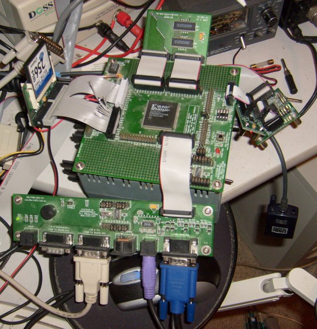
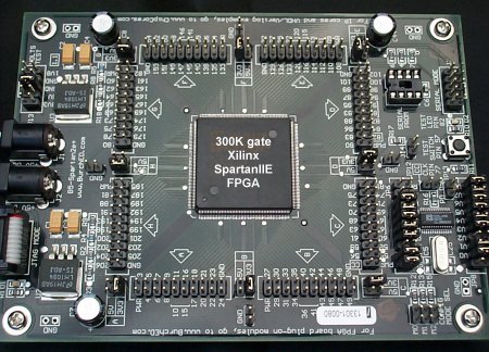
3.1 BurchED B3-Spartan2+ Board
My first FPGA projects used the B3-Spartan2+ board from Burch Electronic Design locate up in Sydney here in Australia. The B3-Spartan2+ used a 200K gate Xilinx XC2S200 and I also used the B3-SRAM 128K x 16bit SRAM module and the B3-FPGA-CPU-IO board for serial communications, keyboard, mouse and VGA video. The B3-Spartan2+ board was replaced by the B5-X300 board which used the larger 300K gate XC2S300E. Neither the B3-Spartan2+ nor the B5-X300 are sold now, although they were sold internationally when they were first introduced.
3.1.1 ICST525-01 PLL Clock divider
The B3-Spartan2+ and the B5-X300 boards both use the ICST525 programmable PLL clock chip for the master clock input with 20 MHz reference clock. By configuring jumpers on the pins of the chip you could select a large range of clock frequencies. There is one of these chips on the main B3 and B5-X300 boards, and one on the B3-FPGA-CPU-IO module. The B5-Peripheral-Interconnect module did not have an ICST525 on it.In some of the early projects I used clocks which are multiples of 4.915254 MHz as it is an exact binary multiple of 9600 Baud used by the MiniUart. More recent projects have been designed for a 50MHz system clock as this appears to be commonly used on other FPGA boards which made it earier to port the designs to other FPGA boards. On the designs using a 50 MHz clock, the baud rate clock is derived from a VHDL pre-scaler.
http://www.idt.com/?app=calculators&device=525_01 Frequency calculator web page
The following two pages have been pre-calculated:4.915254 MHz ICST525-01 for Memio and System68 at 9600 Baud
9.830508 MHz ICST525-01 for System68 at 19K2 Baud.
3.1.2 Notes on modifying the B3-SRAM module
On the original B3-SRAM module there was no separate output enable (OE*) and write (WR*) signals for upper and lower byte control. This was because of the limited number of pins on the adjacent 20 pin headers. To perform byte writes, its was matter of reading the full 16 bits and modifying either the upper or lower byte and writing it back. BurchED fixed the problem on the B5-SRAM module. Tony permanently grounded the Output Enable (OE*) pin of the RAM chip and had a single Chip Select (CS*) and separate upper and lower byte write enables (WEU*, WEL*) which essentially become read/write lines.
I modified my B3-SRAM module by cutting the WE* track to U1 on the top of the board and the OE* to J2 pin 19 on the bottom of the board. I wired U1 pin 12 to J2 pin 19 which becomes WEL* (J2 pin 18 becomes WEU*) and I grounded the OE* signal on pin 28 of U1 & U2. The pin-outs in the ".ucf" file are for my modified B3-SRAM module and you will have to change them to suit the B5_SRAM. Note The address and chip select lines have been resquenced on the B5_SRAM.
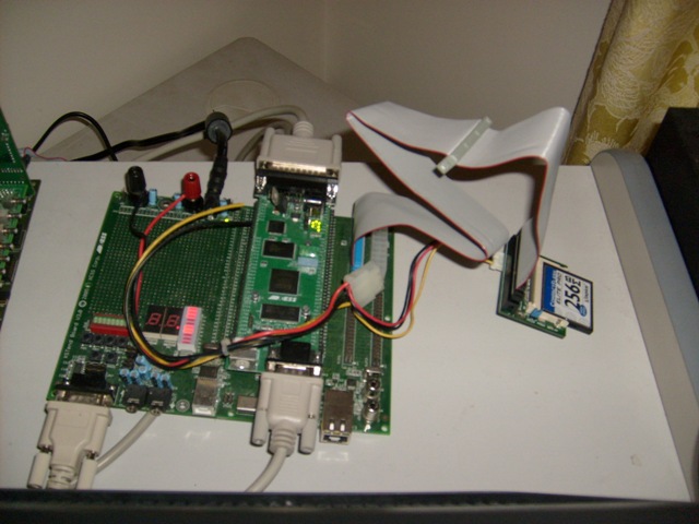
Some of my early designs use the original B3-SRAM module configuration, and some the revised configuration. You will have to check the code to determine which is which.3.1.3 Notes on adding a CF card.
I added a CF card to the B3-Spartan2+ board by using a CF to IDE adapter from Darkwire Pty Ltd (See section 3.5.1). You can see the CF IDE adapter and cable in the photo above. The CF card was used to run the Flex9 Disk operating system using System09 on the B3 board.I cut up a 40 pin IDE ribbon cable and split the cable so that the 16 data pins (IDE pins 3-18) and ground pin (IDE pin 19) on the 40 pin connector go to the bottom 17 pins of a 20 pin IDC connector for J4. Pin 1 of the 40 pin IDE connector (ide_reset_n) was split off the cable and soldered to pin 4 of the IDC connector of J3.
The control signals (IDE pins 1, 21, 23, 25, 27, 28, 29, 31-40) go to the bottom 16 pins of the 20 pin IDC connector for J3. Note that IDE pins 31-40 directly line up with J3 pins 11-20, however the ground pins between remaining control pins on J3 must be cut off and the remaining wires individually lined up on the connector, which can be a little bit fiddly.
I inserted 4 wires on pins 1-3 of the J3 connector. Pin 1, which is the +3.3V supply rail, was soldered to the power connector of the CF IDE adapter. Pins 2 & 3 of J3 were left disconnected and pin 4 of the J3 connector (ide_reset_n) was soldered to pin 1 of the 40 pin IDE cable as previously stated.
#
# B3 Connector J4
# IDE / CF Interface
# Note that this pin out is NOT consistent with the B5-IDE
# It's called the peripheral bus for consistence with the XESS board
#
#NET "+3.3V" #pin 1 (not used)
#NET "pb_gclk2" LOC = "p182"; #pin 2 (not used)
#NET "pb_spare2" LOC = "p160"; #pin 3 (not used)
NET "pb_data<7>" LOC = "p161"; #pin 4 - ide pin 3
NET "pb_data<8>" LOC = "p162"; #pin 5 - ide pin 4
NET "pb_data<6>" LOC = "p163"; #pin 6 - ide pin 5
NET "pb_data<9>" LOC = "p164"; #pin 7 - ide pin 6
NET "pb_data<5>" LOC = "p165"; #pin 8 - ide pin 7
NET "pb_data<10>" LOC = "p166"; #pin 9 - ide pin 8
NET "pb_data<4>" LOC = "p167"; #pin 10 - ide pin 9
NET "pb_data<11>" LOC = "p168"; #pin 11 - ide pin 10
NET "pb_data<3>" LOC = "p172"; #pin 12 - ide pin 11
NET "pb_data<12>" LOC = "p173"; #pin 13 - ide pin 12
NET "pb_data<2>" LOC = "p174"; #pin 14 - ide pin 13
NET "pb_data<13>" LOC = "p175"; #pin 15 - ide pin 14
NET "pb_data<1>" LOC = "p176"; #pin 16 - ide pin 15
NET "pb_data<14>" LOC = "p178"; #pin 17 - ide pin 16
NET "pb_data<0>" LOC = "p179"; #pin 18 - ide pin 17
NET "pb_data<15>" LOC = "p180"; #pin 19 - ide pin 18
#NET "ground" #pin 20 - ide pin 19
#
# B3 Connector J3
# IDE / CF Interface
# Note that this pin out is NOT consistent with the B5-IDE
#
#NET "+3.3V" #pin 1 (wired to the power connector)
#NET "ide_gclk1" LOC = "p185"; #pin 2 (not used)
#NET "ide_spare1" LOC = "p181"; #pin 3 (not used)
NET "ide_reset_n" LOC = "p187"; #pin 4 - ide pin 1
NET "ide_dmarq" LOC = "p188"; #pin 5 - ide pin 21
NET "pb_iowr_n" LOC = "p189"; #pin 6 - ide pin 23
NET "pb_iord_n" LOC = "p191"; #pin 7 - ide pin 25
NET "ide_iordy" LOC = "p192"; #pin 8 - ide pin 27
NET "ide_con_csel" LOC = "p193"; #pin 9 - ide pin 28
NET "ide_dmack_n" LOC = "p194"; #pin 10 - ide pin 29
NET "ide_intrq" LOC = "p195"; #pin 11 - ide pin 31
NET "ide_iocs16_n" LOC = "p199"; #pin 12 - ide pin 32
NET "pb_addr<1>" LOC = "p200"; #pin 13 - ide pin 33
NET "ide_pdiag_n" LOC = "p201"; #pin 14 - ide pin 34
NET "pb_addr<0>" LOC = "p202"; #pin 15 - ide pin 35
NET "pb_addr<2>" LOC = "p203"; #pin 16 - ide pin 36
NET "ide_cs0_n" LOC = "p204"; #pin 17 - ide pin 37
NET "ide_cs1_n" LOC = "p205"; #pin 18 - ide pin 38
NET "ide_dasp_n" LOC = "p206"; #pin 19 - ide pin 39
#NET "ground" #pin 20 - ide pin 40
3.2 BurchED B5-X300-Spartan2e Board
Burch Electronic Design superseded the B3 board with the B5 based around the 300K gate XC2S300E. Like the B3 board the B5-X300 had a number of add on boards such as the B5-SRAM, B5-Peripheral-Interconnect, B5-CF Compact Flash interface, Switch and LED boards. These boards and modules are no longer sold by BurchED and Tony is now focusing on developing FPGA training material. (See section 1).
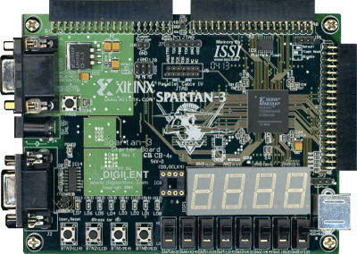
3.3 Digilent Spartan 3 Starter Board
The Spartan 3 starter board, made by Digilent Inc originally used a XC3S200 200K gate device although there is also a XC3S1000 1000K Gate variant available. It has 1MByte of SRAM arranged as 256K x 32 bits. It features VGA connector, RS232 connector, PS/2 Keyboard connector, Push buttons, switches, individual LEDs as well as 4 x 7 segment LED displays. It has 3 x 40 pin expansion connectors for adding on peripheral boards. It also has serial flash for storing your FPGA configuration.
The only real draw back with this board is that there is no program flash memory for mass storage, and there are only 3 bits for the VGA output which means only 8 colours can be displayed unless you add extra DAC resistors.
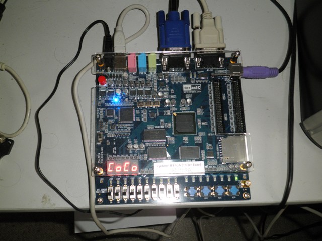
I have implemented System09 on the 200K gate board and it only just fits. For US$109 it is not a bad buy. The XC3S1000 version of the board from Digilent costs an additional US$50 but gives you much more logic. Gary Becker has used the XC3S1000 version of this board to implement early versions of his Tandy Colour Computer 3 on an FPGA.
http://www.coco3.com/community/2009/09/coco3-fpga-project/
http://groups.yahoo.com/group/CoCo3FPGA/
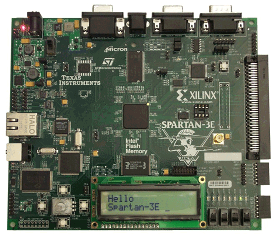
3.4 Digilent Spartan 3E Starter Board
The Xilinx Spartan 3E starter board, also made by Digilent Inc uses a XC3S500E FPGA. It has plenty of features, such as Flash Memory, DDR SDRAM, LCD display, ADCs, DACs, RS232, VGA, Ethernet Phy and much more. It has a number of 6 pin headers for adding small 4 bit modules, as well as a Hirose 100 pin FX2 connector, which can be used for add on boards such as the VDEC-1 Video digitizer.
The limitation of the Spartan 3E start board is that there is no SRAM, which means you need a DDR-SDRAM controller core to use it unless you are using EDK. Also, like the Spartan 3 starter board, the VGA connector only has 3 bits for video (one bit for R,G &B) which means there are only 8 colours. There is a modification on Mike J's FPGA Arcade web site that uses some of the pins on the FX2 connector to extend the VGA colour range to 12 bits or 4096 colours by adding additional resistors.
This board was given to me as part of a project to validate my 6809 design. The 6809 design uses the internal Block RAM to implement 32KBytes of RAM and an 8KByte Program ROM. It would be nice to get a DDR RAM controller working for it.
3.5 XESS XSA-3S1000, XST-3.0 & XSUSB
The XSA-3S1000 board from XESS, as the name implies, uses a XC3S1000, 1 million gate Spartan 3 chip. It has a 9 bit (512 colour) VGA output connector as well as a PS/2 keyboard or mouse connector. It has 32MBytes of SDRAM and 4MBits (?) of Flash. The Flash memory is bank selectable and doubles as a FPGA configuration and program code store.
XESS use a CPLD to act as a download controller which connects to the printer port of your computer. You can download FPGA configuration, Flash Program Code, or SDRAM Code using a suite of software utilities. You can also use the Xilinx Parallel IV pod too if you want. XESS also sell a XSUSB module that allows the board to be programmed over USB. XESS have a lot of free example code for the XSA-3S1000 on their web site as well as a SDRAM controller IP for use with the board.
The other good feature of this board is the large number of header pin outs. The board is actually designed to plug into the XST-3.0 carrier board (the XST-4.0 is the current version), but can be used to interface to your own carrier if you desire.
The XSA-3S1000 board was purchased so a group of internet friends could develop a PDP-8 project. The large number of uncommitted I/O pins made the board ideal to interface to switch banks and LED display panels as well as other PDP-8 bus devices.
3.5.1 IDE Compact Flash Interface.
The XST-3.0 board has an IDE interface for adding a hard disk drive. The 16 IDE data pins and IO read/write pins are also used for the ethernet controller and the two expansion slot connectors. I have used a Dual IDE to CF adapter card which I bought from Darkwire here in Australia. Darwire sell a variety of CF, SATA and SD/MMC to IDE adapter cards, although I have only tried the CF card on the XST-3.0.
The IDE interface on the XST-3.0 and XSA-3S1000 does not have 5V protection so it is important that you power the IDE-CF card from 3.3V. I mounted terminals on the 3.3V supply of the XST-3.0 board and powered the CF card off that. The IDE-CF card uses a 3.5" floppy 4 pin power connector which I chopped off an old PC. The red lead is normally the +3.3V and black leads ground, but you should always check for yourself with information on web to ensure that is correct.
3.6 Memec Design / Avnet V4FX12LC & P160 Analog
The Memec Design V4FX12LC board uses the Virtex 4 FX12 FPGA which includes a 200MHz Power PC 405 processor in addition to about 500K gates of programmable logic. This board was purchased for me by work with the idea of doing GPS receiver signal processing. It was bundled with EDK7.1 and BaseX ISE 7.1 as part of the XFest training course offered by Memec in Australia in 2005.
The board features 64MBytes of 16 bit DDR-SDRAM as well as flash memory, push buttons and an LCD display. Monta Vista provide a version of Linux for the ML302 board which should also run on the V4FX12LC board. It is only a demo version, so you have to pay $s if you want to do any Linux development with it. Also Monta Vista Linux on was designed to run with a soft-core Ethernet controller and does not use either of the two Ethernet controllers built into the V4FX12LC. I believe the Ethernet soft-cores on EDK 7.1 are time limited unless you purchase them.
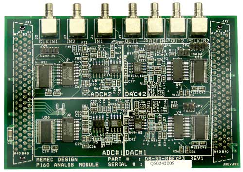
Memec were taken over by Avnet in 2005/6, but last time I saw, Avnet were still offering the P160 add on modules for this board. The Communications 3 module offers SRAM, VGA and PS/2 interfaces, ADCs and DACs as well as communications interfaces. The ADCs and DACs are only useful for audio frequencies however. There is also high speed data acquisition module for a few hundred dollars which work up into the 10s of Msps range.
You can buy a number of commercial cores such as Floating Point Units for the PPC405 for the Virtex 4 but they are too expensive for me. There are FPUs on the open cores web site, but they are not designed to integrate with the APU of the PPC405 to the best of my knowledge. Webpack 8.1 and onwards does include Coregen that includes FPUs, FFTs and so on but I'm not sure how these interface with the PPC405 on the Virtex 4.
It would like to use the V4FX12LC for a software radio:
http://members.optusnet.com.au/vk3biz/gnuradio.html
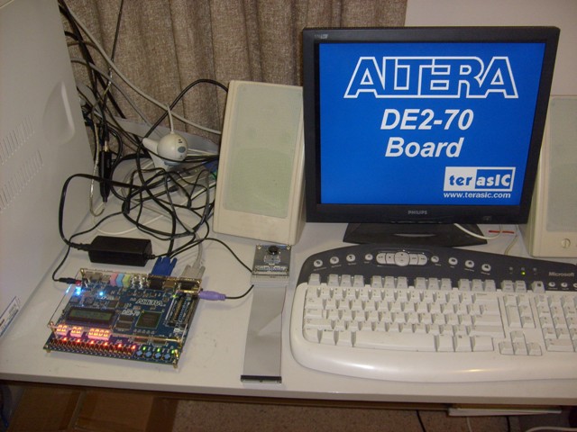
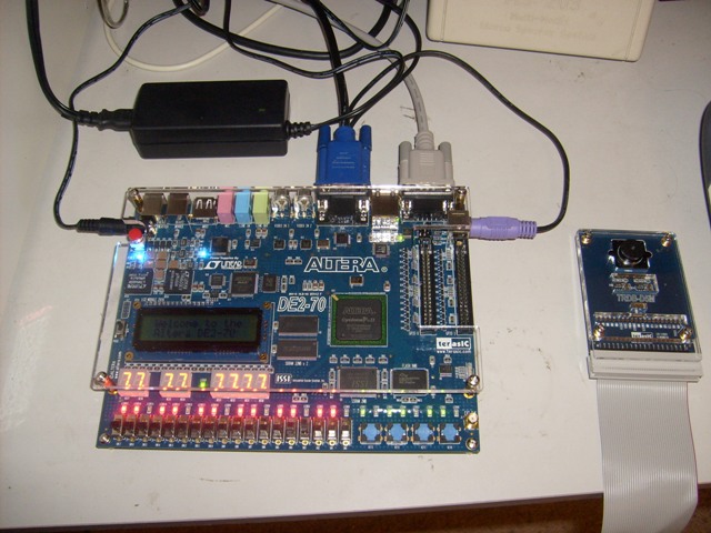
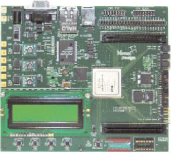
3.7 Altera / Terasic DE2-70 Cyclone 2 & D5M camera module
Altera / Terasic DE2-70 board running the initial demo design.
Close up of the DE2-70 board with the D5M digital camera on the right.
Tuesday 6th April 2010
I have a new toy, a Terasic DE2-70 board with Altera Cyclone II EP2C70F896 FPGA, 64MB SDRAM x 2, 2MB SSRAM and 8BM Flash, Multimedia interface with dual TV decoders. I plan using two D5M 5Mpixel camera sensors (one shown on the right) to do some stereo vision work. The board is shown running the application shipped with the board.
Cornell University runs the ECE 5760 Advanced Microcontrollers class. They use the Altera/Terasic Cyclone II DE2 board (as opposed to the DE2-70). The following link is to their Final Projects. The head tracking project uses use the D5M camera module. In 2010 the projects included a stereo vision depth mapper.
http://people.ece.cornell.edu/land/courses/ece5760/FinalProjects/
3.8 Altera / Terasic DE1 Cyclone 2
Altera / Terasic DE1 board running Gary Becker's FPGACoCo3
Tuesday 18th January 2011
I bought a Terasic DE1 board for running Gary Becker's CoCo3FPGA which uses the CPU from my System09 project but adds the GIME and other support logic such as the keyboard and sound interface. The DE1 board has a Cyclone II 20K LE EP2C20 FPGA, 8MBytes of SDRAM, 512KBytes SRAM, 4MBytes of flash, VGA port, RS-232, PS/2 Port, EPCS4 configuration flash, 2 x expansion headers, 24 bit audio CODEC, 27MHz, 50MHz & 24 MHz oscillators, SD Card socket, Altera USB Blaster controller, 8 green LEDs, 10 Red LEDs, 4 x 7 segment displays, 10 toggle switches and 4 push buttons.
http://groups.yahoo.com/group/CoCo3FPGA/
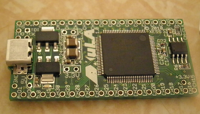
3.9 XESS XuLA Spartan 3A
Friday 28th January 2011
Dave vanden Bout sent me a complementary version of his XuLA Spartan 3A 200K gate board. http://xess.com/prods/prod048.php
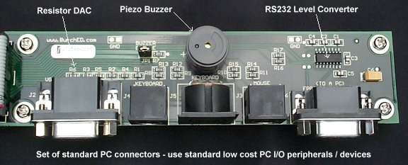
I have a few old B5 peripheral connector boards that I intend to use to interface to it. The B5 peripheral interconnect boards have an MAX3232 RS232 level converter on it as well as PS/2 keyboard and mouse connectors and a 6 bit VGA resistor DAC (2 bits for each R, G and B signal).
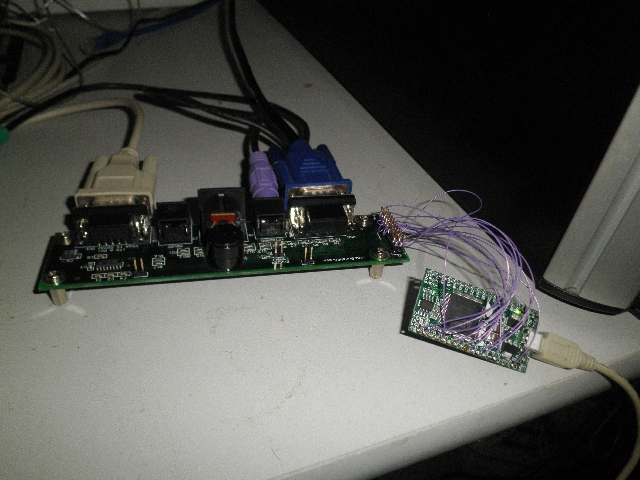
Sunday 5th June 2011
I did get System09 running on the XuLA board. I used wire wrap wire on the B5-Peripheral-Connect board and soldered them to the pins of the XuLA board. I've yet to upload the design files to opencores.org. It only uses half of the SDRAM data bus, and memory is limited to 1MB by the configuration of the DAT.
4. FPGA Design Tools
4.1 Xilinx Web Pack ISE:
The Web Pack ISE design software is available free from Xilinx. The latest versions are around 3GB or so you need a fast internet connection if you want to download it. Alternatively you might want to send off for a DVD from Xilinx. Old versions of the Web Pack ISE software I think are still available on the Xilinx web site.
Most of the project on this web site are hosted on opencores.org due to the limited amount of space on this web site. The Xilinx WebPack ISE software is constantly being updated, so some of the project files on this web site may be out of date. WebPack ISE should update the project file, but if it is too old, then you may need to rebuild it for your version.
4.2 Altera Quartus:
Altera provide Quartus II software for development work with their FPGAs. I have used Quartus II for the System09 implementation on the DE1 board. The first book I bought for learning VHDL was simply called "VHDL" and was written by Douglas Perry. The book used the Altera software for examples. Altera were the first to make their software free I believe and Xilinx came to the party shortly after.
5. FPGA Projects:
5.1 System16 - My Initial VHDL CPU Project
System16 is only a paper design and is a combination of a 6809 design and a sort of striped down 68000, in terms of the number of registers, addressing mode terminology and bit operators. It was more an exercise in designing a 16 bit CPU for memory that did not have byte access.
5.2 Memio.zip Memory I/O Tool
Memio is a state sequencer for examining and modifying RAM on the B3-Spartan2+ board. It was one of my first projects as you can probably tell from the VHDL code. It was a matter of getting something up and running quickly that allowed me to check the functioning of the B3-SRAM. These days it is so easy to get a microprocessor running with a monitor program that this project is a bit redundant but I have kept the design here as a historic record of my work.
It was developed using Xilinx WebPack ISE 4.2 VHDL tools. It uses a highly hacked version of MiniUart by Ovidiu Lupas which used to be on www.opencores.org
Memio assumes you have the B3-FPGA-CPU-IO card connected to connector J3 and the B3-SRAM card connected to J6 and J9. The current clock divider for the UART assumes a 4.915254 MHz clock for 9600bps serial I/O, which gives a nice round division factor for the clock divider.
Commands for Memio are:
M <address> Examine memory location <space bar> <data> Write 16 bit hexadecimal value N Display Next memory location P Display Previous memory location For simplicity only the first 64Kwords of SRAM are used (128Kbytes). Address line A16 is grounded. Data words are 16 bits wide. Command keys and hexadecimal values must be all uppercase (although that could easily be changed). All input characters are echoed back out the UART. This is because I could not get Hyperterm to echo characters locally under windows98 SE.
5.3 Micro8 - A very simple microprocessor
Micro8 was based on a minimal set 4 instruction computer by Tim Boscke which was designed to fit in a 32 Macrocell CPLD. Tim's design is now available on the Opencores web site as the MCPU (Minimal CPU) project. http://www.opencores.org/project,mcpu The whole MCPU design fits in a single page.
Tim's computer had only ADD, NOR , STA and JCC instructions and could only address 64 bytes of memory. It had a single carry bit which was set by the JCC (Jump on Carry Clear) instruction. Most basic microprocessor instructions can be built up using these four basic instructions.
For my Micro8 design I have added an 8 bit index register and four addressing modes, Immediate, Absolute, Indexed and PC Relative and I've extended the addressing range from 64 bytes to 2K bytes. The top five bits of the opcode byte determine the operation and addressing mode. The bottom 3 bits of the opcode form the high bits of the address argument. I've also added a Zero (Z) Flag and a Negative (N) flag and conditional branches that do not change the condition codes. Micro8 does not have a return stack and does not support subroutine calls.
Micro8 was implemented on the B3 Spartan2+ board. Although I have included the B3-SRAM in the I/O pin-outs, it does not use the SRAM to print the message. The VHDL code should run quite happily without the B3-SRAM module. I put the I/O interface module on connector J3 of the B3-Spartan2+ board, but its probably better suited to J8.
5.4 Micro8a - Adding a Stack
In my Micro8A I have added a 7 bit stack pointer at $0FF that works down to $080. I've added subroutine calls, Push and Pull registers and interrupts as well as some inherent single byte instructions to operate on the accumulator and index register.5.5 Micro16 - Very Basic 16 bit CPU
Micro16 has 8 instructions and two addressing modes: Direct and Indirect. Direct addressing can address 4K Words of Data or Program space while indirect addressing can address 64K Words of data space. The instruction word is 16 bits wide, with 3 bits used for the instruction, 1 bit used for the addressing mode and 12 bits used to form the Direct address. It has an 8 level hardware stack and one interrupt input. It was intended as a substitute for a compact flash state machine. So far I have not managed to get it to work with the Compact Flash, which is a bit unfortunate given how simple it is. I think the problem may have something to do with the speed at which it accesses Compact Flash.5.6 Micro16 - Processing Array
The idea was to implement an array of Micro16 computing elements with shared block RAM memory.
5.7 Motorola 8 bit CPUs
I have coded some of the Motorola 8 bit CPUs, namely the MC6800 and MC6801, MC6805, MC6809 and MC68HC11. These are still works in progress and I have kept a record of their development on their respective web pages.
I originally attempted to use the 6809 VHDL design by Flint Weller as a starting point, but it was a bit too complex and too ambitious a project for someone just starting out. For newbies just starting out on VHDL and FPGA design I'd recommend starting with something simpler like the Micro8. You can find Flint's VHDL core on the Flex User Group page under "File Exchange" however it needs a lot of work.
It was the ambition of one of the Flex User Group members to design a FPGA based Flex system. FLEX is an old disk operating system for the 6800 and 6809. The 6800 and 6809 can only address a maximum of 64KBytes of memory although with the SWTPc 6809 it was extended with what they called a DAT or Dynamic Address Translation, that can map 4K blocks from 1MByte of memory into the 64K addressing space.Since Flint Weller's 6809 design was too complex to understand, and I think was only intended for simulation, I went back to basics and designed the Micro8, System05 (a 6805 which I still have not completed), System68 (a 6800), System11 (a 68HC11 which is still not finished) and eventually I worked my way up to System09 which is a 6809 System On a Chip. System09 emulates the SWTPc hardware.
The "System" name was all I could think of at the time and refers to a Systems On a Chip since the design includes peripherals such as ACIA (UART), VDU, PS/2 Keyboard, Dynamic Address Translation, Timers, Parallel I/O etc. as well as the CPU cores. A number of people are using System68 and System09 CPU cores as the basis of pinball and arcade games. See the resources links below for more details.
I have managed to get the Flex 9 Disk operating system running on System09 using a RAM disk and Compact Flash card configured for True IDE mode. Boards with IDE interfaces such as the XESS XSA-3S1000 with XST-3.0 motherboard will operate with a IDE to CF adapter as well. Flex 2 is also available for the 6800, however I have not managed to modify the disk drivers for that yet.The Flex Users Group has collected most of the old FLEX Software and SWTPc documentation and have archived it. Much of the Flex software was obtained from that archive. If you have any old Flex software, I'm sure the Flex User Group would be interested to hear about it.
5.8 System01 - 6801 - Working (Incomplete I/O)
5.9 System68 - 6800 - Working
5.10 System05 - 6805 - Work in Progress
5.11 System11 - 68HC11 - Partly Working
5.12 System09 - 6809 SOC - Runs Flex9 with VDU and PS/2 keyboard
System09 has been ported to the following Xilinx FPGA development boards:
- BurchED B3-Spartan2+
- BurchED B5-X300
- Digilent Spartan 3 starter board
- Digilent Spartan 3E starter board
- XESS XSA-3S1000 and XST-3.0 carrier board
- XESS XuLA 200 with interface board
System09 has also been ported to the Terasic DE1 board using Altera's Quartus II software.
Recent versions of Xilinx Webpack ISE development software no longer support the Spartan 2 and Spartan 2e devices used on the BurchED B3 and B5 boards.
5.13 System6801 - Wishbone Compliant 6801 for Altera by Michael L. Hasenfratz Sr.
Michael L. Hasenfratz has taken my System01 core and has made it wishbone compliant. He has also added some of the 6801 peripherals at locations $0000 to $001F. The project is being hosted on the OpenCores web site. He has ported it to an Altera FPGA.
Michael has kindly made his Relocatable Macro Assemblers and Linker for the MC6800, MC6809 and MC68HC11 available to the public (as shareware ?). It can be down-loaded here:
RMCAXX.zip
6. VHDL & Verilog IP Resource Links:
http://www.opencores.org Open Cores Repository.
The Open Cores web site is the main web site for open source FPGA cores.
http://www.fpgacpu.org Jan Gray's Risc CPU Web Site
Jan Gray has a XR16 RISC CPU , GR000 RISC CPU and XSOC (System on a Chip). He also runs the FPGA CPU mailing list.
http://www.fpga-faq.com/ Philip Freidin's (Fliptronics) FPGA FAQ.
The FPGA Frequently Asked Questions web site.
http://tech.groups.yahoo.com/group/FPGA_CV/ FPGA Computer Vision
A list I set up to discuss the use of FPGAs for Computer Vision applications
http://instruct1.cit.cornell.edu/courses/ece576/FinalProjects/ Cornell University ECE5760 Advanced Microcontrollers Final Projects
Lots of interesting student projects with demonstration videos.
http://groups.yahoo.com/group/CoCo3FPGA/ Gary Becker's CoCo3 on a FPGA Yahoo Group
Gary Becker is using the CPU from the system09 project for his CoCo3 (Tandy Colour Computer 3) on an FPGA.Gary first ported his CoCo3FPGA project to the XC3S1000 Digilent Spartan 3 starter board but is now mainly using the Terasic DE1 board.
http://www.youtube.com/watch?v=E7982JhI5Kc
Youtube video of Gary's CoCo3FPGA at the Glenside CoCo Fest 2010 as implemented on an Altera DE1 board
Glenside CoCo Computer Club who host the CoCo Fest.
http://www.edcheung.com/album/album07/Pinball/wpc_sound.htm Edward Cheung's Williams Pinball Controller page
Edward is using CPU09 core with a Digilent Spartan 3A board to implement a Williams Pinball Controller.
http://members.iinet.net.au/~msmcdoug/ Mark's Perpetually WIP Home page
Mark McDougall's Vic20, ZX81, TRS80 and Arcade game web page.
http://pacedev.net/ Programmable Arcade Circuit Emulation.
Forum for FPGA arcade game developers.
http://www.fpgaarcade.com Mike J's FPGA Arcade.
Mike Johnson's complete PACMAN, Space Invaders, and Galaxians in FPGA !
http://www.itee.uq.edu.au/~jwilliams/mblaze-uclinux/ John Williams MicroBlaze uCLinux Web Site.
John Williams is a Professor at the School of Information Technology and Electrical Engineering at the University of Queensland. He runs quite an active mailing list for implementing uCLinux on the Xilinx MicroBlaze soft-core processor.
http://www.c-to-verilog.com/ C to Verilog - Automating Circuit Design
C-to-Verilog is a free service for circuit designers.
http://excamera.com/sphinx/fpga-vhdl-verilog.html James Bowman's project page
Verilog examples, home-brew Forth CPU and NTSC composite video generator..
http://excamera.com/sphinx/gameduino/ James Bowman's Gameduino.
Sprite controller for tiny microprocessors such as the Atmel AVR.
http://www.birdcomputer.ca/ Robert Finch's Bird Computer - FPGA Cores
Robert has a variety of CPU, video, audio, timekeeping and keyboard projects for download on his web site.
http://www.ht-lab.com/freecores/cpu8086/cpu86.html
CPU86 8088 Free FPGA IP Core
HT-LAB FPGA / VHDL / SystemC / Embedded
Various FPGA projects for the hobbyist. Includes information for connecting devices such as LCD Displays and R/C Servos to FPGAs.
http://alexfreed.com/FPGApple/ Interfacing Compact Flash to the Spartan 3 Starter Board
Alex has used a Spartan 3 starter board to implement an Apple II. He has used a Digilent Test Point Header board to connect an IDE CF adapter.
http://www.retromicro.com Doug Hodson's Web Page
Doug has implemented a few projects using the XESS XSA100 FPGA Board. Doug's project page has some examples of VGA video generators. The XSA100 is quite a nice board with Flash memory and Dynamic RAM, although it uses a smaller FPGA and access to static RAM conflicts with some of the I/O pins. The XSA100 uses a XC2S100 FPGA and can be purchased with the XStend prototyping motherboard. For more details check out http://www.xess.com . They have all the manuals on their web site. The XESS documentation is quite good.
http://www.madscientistroom.org/fpga/ Randy Thelen's Mad Scientist Room.
Randy Thelen has a good User Constraint File generator amongst his FPGA bits and pieces.
http://www.6502.org/users/dieter/index.htm Dieter's Homebuilt CPUs.
http://brainwagon.org/ Mark VandeWettering's Homebrew computing and logic blog.
http://www.cs.ucr.edu/~dalton/i8051/
The Dalton Project at the University of California Computer Science Dept in Riversdale have an Intel 8051 core. There is a synopsis model as well as C++ simulator for the 8051.
http://www.dte.eis.uva.es/OpenProjects/OpenDSP/index.htm
The Department of Electronic Technology at the University of Valladolid in Spain have an Open DSP design which can be found on their web site.
http://tech-www.informatik.uni-hamburg.de/vhdl/vhdl.html
University of Hamburg VHDL Page. Assorted VHDL tools and microprocessor cores.
http://www.opencores.org/project,tv80
Daniel Wallner's PPX16 (PIC16C55, PIC16F84)
http://www.opencores.org/project,t51
Daniel Wallner's T80 (Z80) (actually it's the TV80)
http://www.opencores.org/project,ax8
Daniel Wallner's AX8 (90S1200, 90S2313)
http://www.opencores.org/project,t65
Daniel Wallner's T65 (6502)
http://www.opencores.org/project,ppx16
Daniel Wallner's PPX16 (PIC16C55, PIC16F84)
K Ring Technologies Semiconductor Indi16 16n bit Forth CPU. Designed for Altera Quartus II software.
http://www.gmvhdl.com/downloads.html
Green Mountains Computing Systems have a MC68HC11 VHDL core as well as VHDL tools and simulators. I tried compiling this core under the Xilinx ISE 4.1 Webpack software and it used 200% of the XC2S200 resource, so it is not an efficient design. Later versions of Xilinx ISE Webpack may be more efficient.
http://www.mcmanis.com/chuck/robotics/fpga/index.html
Chuck McManis has put up a web site with a list of his projects for the B3-SPARTAN2+ board.
http://zxgate.sourceforge.net/
For some fun, projects on the net, using Z80 cpus implemented completely in the FPGA. Daniel Wallner's computers using FPGA T80 cores .

Home