|
[Technology Report]
New Breed Of ASICs Melds The Best Of Two Worlds
Thanks to faster turnaround times and lower development costs than full custom ASICs, platform/structured ASICs bring stiff competition to FPGAs and ASICs.
Dave Bursky
ED Online ID #7547
March 15, 2004
Over the last half decade, a new class of configurable ASICs has made inroads by bridging the performance and cost gap between designs based on full custom ASICs and high-density FPGAs. Known as platform and structured ASICs, these system-on-a-chip (SOC) solutions cull some of the best aspects of both custom ASICs and FPGAs. As a result, designers have a quick time-to-market option that features lower development costs than ASICs and higher performance and often lower unit costs than FPGAs
(Fig. 1).
Figure 1
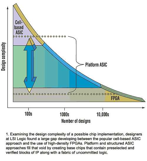
Depending on the number of metal layers, structured/platform ASICs could require just two to six weeks to produce once the RTL description is completed. In contrast, a full ASIC design might require five or more months to produce a similar chip once the RTL is completed. High-end FPGA-based designs often require more time than structured ASICs due to extra analysis often needed for timing closure and routing.
Many designers use the terms platform and structured ASIC interchangeably, and at the most general level, the two approaches are very similar.
(For an overview of designing with platform and structured ASICs, see the Basics of Design on Platform ASICs, p. 64A, this issue.)
About a dozen vendors currently offer many varieties of platform and structured ASIC solutions. They fall into several groupings, the largest of which consists of companies that provide pre-manufactured silicon customized with one or more layers of metal interconnect. Suppliers in this group include Altera (the HardCopy version of its FPGA), AMI Semiconductors (Xpress Arrays), Chip Express (CX4000 and 5000 families), eASIC (eASIC Array), Faraday Technology (a metal programmable cell array), Fujitsu (AccelArray), Lightspeed (Lightning and Luminance families), LSI Logic (RapidChip family), and NEC (ISSP series).
Another company joining the fray comes from the FPGA side. Leopard Logic has just released the Gladiator family, which combines both metal-mask and RAM-based configurable logic blocks and other resources, all on one chip. Previously, the company supplied intellectual property (IP) consisting of RAM-based configurable logic.
A second group consists of what the industry calls soft IP platforms. In this group, no silicon is premanufactured. Rather, IP blocks are selected to form a system solution minus the customer's unique logic and then prequalified. The selected and prequalified blocks are solidified as an RTL description, which can then be quickly merged with the unique RTL logic defined by the customer. Companies offering such options include Atmel, eSilicon, LSI, PalmChip, and Toshiba. These solutions permit more customization because the RTL files can be edited to delete undesired functions. Yet NRE charges are higher than they are for the pre-manufactured choices since a full mask set must be created after finalizing the RTL description.
With all of these potential solutions, the old adage "the devil is in the details" aptly applies. Although most prefabricated silicon offerings have similar collections of resources - a logic fabric to host the soft IP, dedicated IP blocks such as memories, phase-locked loops (PLLs) and/or delay-locked loops (DLLs), and various I/O ports—there are differences. In some of the more feature-rich versions, you also will find dedicated CPUs, high-speed serializer-deserializers (SERDES), and still other complex functions that make sense to embed in the silicon.
But when you start looking closer, you will find significant differences among the logic fabrics. Some will be implemented from simple gate building blocks similar to the basic gate structures found in gate arrays. Although such fabrics provide the most efficient implementation for the logic and often the best performance, they require as many as five levels of metal to define the logic. Consequently, the mask charges may be a little higher than they are for structured ASICs that need only one or two levels of metal.
A few structured-ASIC logic fabrics take an alternate approach. This method uses more-complex logic cells that are somewhat like cells used in FPGAs. These cells can be configured with just one or two levels of metal. Chips using this approach might have lower non-recurring engineering (NRE) charges. But the logic cells are less efficient from a usage point of view because some logic implementations won't use all of the logic in each cell.
Within the group of pre-manufactured silicon offerings, it's possible to further subdivide the choices into perhaps two categories: basic and advanced implementations. Basic versions pack a minimal set of resources on-chip, typically consisting of the logic fabric, some memory, some PLLs or DLLs, and standard I/O cells. These implementations are usually called structured ASICs.
The more feature-replete versions typically include embedded IP blocks that support DSP operations, CPUs for control-plane applications, multigigabit SERDES channels for high-speed communications, and/or still other large blocks of IP. Such chips are frequently categorized as platform ASICs. That's because the more-complex features may often target a specific group of applications-data communications, networking, or multimedia, for example.
DIG INTO THE DETAILS
Structured and platform ASICs are available in a wide range of processes, from commodity 0.25 µm (250 nm) to the latest 0.09-µm (90 nm) processes, depending on the vendor. Companies such as Fujitsu, LSI Logic, and NEC offer the latest processes, while most of the remaining companies are at 130, 180, or 250 nm. Most of these companies, though, plan to migrate their structured architectures to 90-nm processes by 2005.
Positioned at the leading edge of the structured side are Fujitsu and NEC. Both have 110-nm and smaller implementations that provide designers with up to 3.4 Mgates and functions such as 3.125-Gbit/s high-speed serial interfaces.
Fujitsu's AccelArray CA91 series, featuring 110-nm design rules, is a family of five base chips that use three levels of metal to perform the final configuration. The largest family member, the M50, supports up to 3.4 million system gates, 4.55 Mbits of static RAM, and up to 1176 I/O cells
(Fig. 2). The smallest entry, the M10, has 455k system gates, 860 kbits of SRAM, and 472 I/O cells. The company also developed a vertical-market platform version that includes high-speed serial channels for multigigabit data transfers. Ultra-high-pin-count flip-chip BGA packages with up to 1681 contacts are available to support I/O-intensive applications.
Figure 2
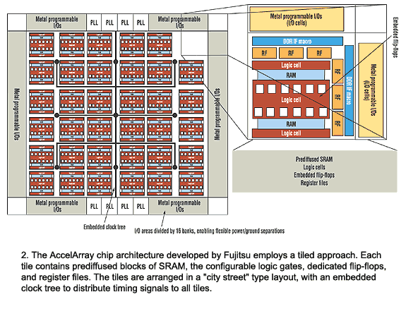
The structured arrays use a total of six levels of metal wiring but are only pre-manufactured through the first three levels. The final three are determined by the system designer's logic that's configured in the logic fabric. The company also plans to offer mask-less configuration using electron-beam lithography. This could help reduce NRE costs and time to production.
The basic logic tile in the logic fabric consists of a block that contains embedded dedicated flip-flops, logic gates, and pre-diffused blocks of RAM. Register files and a double-data-rate (DDR) memory interface macrocell are prediffused blocks of IP in the channels surrounding the array of tiles.
Logic functions implemented with the tiles can operate at up to 333 MHz. Eight analog PLLs, each able to operate at up to 800 MHz, enable designers to divide the logic into as many as eight independent clock domains. Metal programmable I/O cells around the chip's perimeter provide interfaces to standard TTL and CMOS logic levels, as well as P-CML, LVDS, PCI, HSTL, SSTL-2, and others.
NEC leveraged its 90-nm process technology to create a family of seven base chips in its Instant Silicon Solutions Platform (ISSP90) series. The new platforms incorporate the company's experience gained from its first-generation ISSPs released in 2002. Usable gate capacities on the ISSP90 chips range from 1.8 million to 6.5 million, while embedded SRAM bits range from 1.8 to 11.5 Mbits. Unlike most other solutions, though, NEC designers didn't go the linear-progression route, whereby as the gate count goes up so does the SRAM. Rather, they tried to strike a balance of logic and memory that would be most appropriate for several projected applications. Thus, the 1.8-Mgate chip packs 2.7 Mbits, the 2.3-Mgate chip has 1.8 Mbits, another version with 2.3 Mgates contains 11.5 Mbits for memory-intensive applications, the 2.7-Mgate chip holds 7 Mbits, and so on.
Like the Fujitsu chips, the ISSPs also include analog PLLs. But instead of special interface macrocells, the ISSPs include DLLs to distribute timing signals. Circuits implemented in the logic can achieve system clock speeds of up to 350 MHz.
Also incorporated are six to seven levels of copper metallization with low-k intermetal dielectric layers. The lower three levels of wiring predefine interconnections to the embedded IP cores, built-in test logic, clock domains, and power. The next two are the customer-defined connections, and a sixth, common layer reinforces the power grid. When flip-chip packages are required, a seventh layer is used.
The ISSP90's basic architecture is very different from the Fujitsu offerings. Rather than use large tiles of basic logic gates, the logic fabric consists of complex multigate cells. Boundary scan, built-in self-test logic, and test buses are embedded in the logic fabric, along with blocks or single- and dual-port RAMs (512 words by 36 bits) and DLLs.
High-speed serial channels are available on the company's ISSP-1 and ISSP90 families, and still higher-speed serial links capable of 10-Gbit/s transfers are on the drawing boards for future ISSP90 members. Samples of the first ISSP90-series devices are slated for May.
One of the broadest families of base chips can be found in the RapidChip series from LSI Logic. The company offers over 20 different versions, some generic and others market-segment-optimized by incorporating application-specific blocks of IP. But all of the chips employ seven levels of copper interconnect and low-k dielectrics. The logic fabric is based on optimized N- and P-channel transistor pairs, giving designers up to five of the seven levels of metal to customize.
Available in 180-nm design rules, the Foundation series includes 13 members that pack usable gate counts from 700k to 2.8 million and a hierarchy of blocks of single and dual-ported SRAMs totaling from 600 kbits to 2.2 Mbits. Several of the chips include ARM926 32-bit RISC CPU cores, 3.2 Gbit/s SERDES channels, and from 304 to 635 I/O pads. StreamSlice, the series' high-end chip, packs 2.8M usable gates, 2.2 Mbits of RAM, a dozen 3.2-Gbit/s SERDES channels, 80 DDR physical-layer (PHY) bits, 40 HyperPHY channels (gigabit/s-capable), six configurable PLLs, and 486 configurable I/O pads.
GOING TO EXTREMES
Two additional series, the Xtreme family and the Integrator family, are fabricated with 110-nm design rules. The Integrator family has seven members that pack from 2.4M to 7M usable gates and from 1.1 to 3.7 Mbits of SRAM. CPU cores such as the ARM926 or the MIPS 4KEc are available as firm IP that can be placed in the logic fabric. Wirebonding is typically used to attach devices in 252- to 1152-contact BGAs.
The Xtreme family, targeted at higher-performance applications, is optimized for flip-chip BGA packaging to improve the I/O performance. The chips in this family pack from 1.2 to 2.5 Mgates and from 1.6 to 2.1 Mbits of total memory. Additional resources on the Xtreme series include from four to 32 of the company's GigaBlaze multigigabit/s SERDES channels, multiple channels of its HyperPHY SERDES to implement Rapid I/O and other gigabit-speed interfaces, and 40 to 72 PHYs to implement DDR memory interfaces.
Two families of structured solutions are available from Lightspeed Semiconductor. The recent Luminance family is fabricated with 130-nm design rules and offers densities from 250k to 10M ASIC gates and up to 5 Mbits of embedded SRAM. The previous Lightning family is based on 250-nm design rules and offers from 40k to 894k available gates and from 80k to over 900 kbits of embedded SRAM. System speeds up to 200 MHz are possible with the Lightning family, while the Luminance family can run at clock speeds of up to 700 MHz. Both families are based on a configurable logic fabric composed of logic modules, each of which contains separate combinatorial and sequential elements. A single layer of metal is used to configure the logic on the Lightning family devices, while two custom metal layers are used on the Luminance chips.
Well known for FPGA to ASIC conversions, AMI Semiconductor is trying its hand in the structured-ASIC market with the XpressArray and XpressArray-HD families. The HD series includes eight base chips implemented with 180-nm design rules that offer between 64k and 2.6 Mgates, up to 200k internal registers, and up to 1.4 Mbits of embedded SRAM. The previous family also has eight base chips, but with lower logic gate counts that range from 49k to 1.7 Mgates. The logic fabric consists of a sea of macrocells rather than basic gates, so only two levels of metal are needed to configure the chips. This also keeps the NRE charges low. Fees are as little as $80,000 to $200,000.
Structured ASICs from eASIC also weave a macrocell approach into the logic fabric. They come in either a 180-nm six-level or a 130-nm seven-to-eight-layer metal process. The eCell macrocell consists of a RAM-based logic lookup table that feeds a D-type flip-flop
(Fig. 3). The customized metal layers perform the interconnections between eCells. Multiple eCells (2048) are grouped into a block called an eASICore, and the eASICores are tiled across the chip to form the logic fabric.
Figure 3
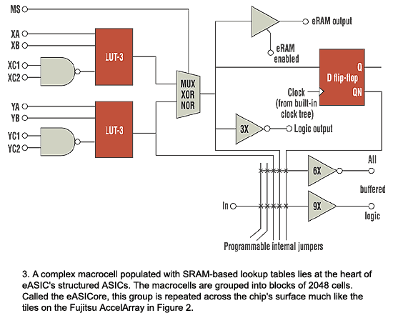
Each eASICore, which is approximately equivalent to 25 kgates, occupies an area of 0.43 mm
2 when implemented with 130-nm design rules. To configure the chip, designers use a single-via mask for the routing and a bit stream that's loaded into the LUT RAMs to define the logic. The single-via customization can be done either with a single mask or even with no masks by using direct-write ebeam lithography. Other resources include blocks of SRAM, a clock distribution network with PLLs and DLLs, and programmable I/O cells.
By combining the best of FPGAs and standard cells, the eASICore fabric delivers the low development cost and short turnaround times associated with FPGAs as well as performance and low production-unit costs that resemble standard cell solutions. The eASICore also is available as a block of IP that designers can license for use in custom ASICs using 180-, 150-, and 130-nm design rules.
Leopard Logic combined metal-mask configuration and programmable complex logic cells to deliver a series of five chips in its Gladiator family. The Gladiator structured ASICs pack from 1.6 million to 25.6 million system gates (about 200k to 3.2M ASIC gates). The chips also include dual multiplier-accumulator blocks, 18 on the smallest chip and 256 on the largest, as well as four, eight, or 16 PLLs and DLLs.
The logic fabric consists of metal-mask configurable logic blocks and RAM-based configurable blocks. Both share an identical logic architecture, but the metal-configurable versions eliminate space-consuming SRAM cells, which saves a considerable amount of chip area.
(For more about the Gladiator series, read "Configurable Logic Solutions Wed FPGA Flexibility With ASIC Efficiency," Feb. 16, p. 38.)
The first chip to be sampled is the CLD6400. It squeezes in 6.4 million system gates, 2.5 Mbits of RAM (64 dual-port RAM blocks, each 1 kword by 36 bits), 64 18- by 18-bit multipliers for a total throughput of 32 GMACs/s, 16 PLL/DLLs, and 472 I/O pads. NRE costs including samples are $50,000.
Three families of structured ASICs, each using a simple base logic architecture, come by way of Chip Express. The ASICs are based on 180-, 250-, and 350-nm design rules - the CX5000, 4000, and 3000 families, respectively. The CX3000 series features usable logic gate counts of 21 to 200 kgates and from 16 to 352 kbits of SRAM. The CX4000 chips pack from 40 to 550 kgates and 64 to 448 kbits of SRAM. The high-end CX5000 series ranges from 44k to 1.8 Mgates and up to 2.6 Mbits of SRAM. This family targets low-power applications, as the logic gates consume just 40 nW/MHz. Only two levels of metal are needed to configure the logic.
Faraday Technology's low-cost family of structured ASICs comes on processes ranging from 350 nm down to 90 nm. The metal-programmable cell arrays offer from 2000 to 10 million equivalent ASIC gates. Seven levels of metal are used. The first three levels deal with general configuration, the next three customize the array with the user-defined logic, and a seventh layer takes on power distribution.
Last but not least are the "soft" RTL platform solutions from Atmel, Palmchip, Toshiba, and others. While these platforms require full mask sets, which doesn't necessarily make them a low-cost option, they offer much faster turnaround times for complex custom designs because a significant percentage of the logic is predesigned and verified. Only the customer-unique portion of the logic must be synthesized, verified, and then merged into the RTL files of the platform supplied by the ASIC vendor.
PalmChip offers several different platforms. The GreenLite IIS solid-state disk controller includes all of the functions needed to form a PCMCIA-based flash-card drive. Based on the company's CoreFrame SoC integration architecture, the platform can be added, or features can be removed, to customize the platform to the desired application.
Also available are the GreenLite IIP portable disk controller, the AcurX configurable SoC platform, and the PalmPak Platform. The GreenLite IIP provides all control functions for a low-power mechanical disk drive. Like the IIS, it can be customized by the designer.
The AcurX and PalmPak are configurable platforms that contain all of the peripheral functions commonly used in an SoC. Designers can select from the company's IP library to add the remaining functions needed to complete the system (the CPU, an Ethernet MAC, an IDE host controller, USB 1.1, and 2.0 interfaces, and many others).
Toshiba's SoCMosaic approach starts with a prequalified collection of IP configured into a generic platform that includes both hardware and software support. Differentiating IP can then be added to customize the platform for a specific application. Toshiba estimates that by using the platform, time-to-market for a customized solution can drop to as little as six months, yet it will perform like a full ASIC.
ASIC suppliers like Atmel and LSI Logic can also prepare soft IP platforms, which collect various IP blocks and preverify their interoperability. Yet these soft IP platforms still cost more and take longer to get to market than the structured, prefabricated solutions.
|
|
|
 |
Copyright © 2004 Penton Media, Inc., All rights reserved. |
|