![]()
|
|
![]()
Hybrid process converts FPGAs to structured ASICs
By Bob Kirk, EE Times
February 12, 2004 (7:51 AM EST)
URL: 원본 문서는 여기를 클릭하세요...
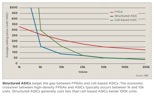
As digital systems have grown more complex, many designers in the communications, computing, medical and industrial markets have turned to programmable-logic devices to prototype their ASICs. Meanwhile, the cost and design cycle time to develop advanced cell-based ASICs continue to grow, making cell-based ASICs an impractical solution for many applications. In response to the growing gap between FPGAs and cell-based ASICs, structured ASICs have emerged, offering a lower cost and faster design cycle times. This article discusses structured-ASIC applications for FPGA prototype conversion.
Due to their programmable nature, FPGA logic makes inefficient use of silicon area and is low in performance compared with ASIC technology. FPGA vendors strive to overcome these limitations by driving IC process development to obtain higher logic capacities and performance. In their quest for higher performance, FPGAs burn significant amounts of static and dynamic power. Fortunately, advanced processes reduce the operating voltage, somewhat mitigating dynamic-power consumption.
Another approach to boost silicon area efficiency is to embed functions in the FPGA fabric. Modern FPGAs support abundant RAM, multipliers, timing generators, processors and I/O features. The fact that most applications use a subset of these functions in a "one size fits all" architecture is just one of the many reasons FPGAs are more expensive, even in volume production.
Converting an FPGA to an ASIC can reduce costs significantly. However, advanced process technologies are usually overkill because the ASIC is typically pad- or package-limited. On top of this, ultradeep-submicron (UDSM) design problems such as signal integrity, on-chip timing variation and timing closure are more challenging, and tooling costs are rising astronomically.
One solution is to use a less aggressive process technology for FPGA-to-ASIC conversions. Mature processes are less expensive because they are well down the learning curve and equipment is depreciated. The main problems are operating-voltage compatibility, maintaining good performance and reducing power consumption. The ultimate solution is to have the voltage, performance and power consumption properties of advanced processes, but with nonrecurring-engineering expense (NRE) and design cycle times of mature technologies.
Hybrid process
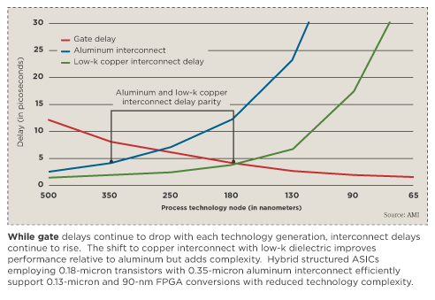
Designing ultradeep-submicron ASICs is not only getting more expensive, but also more complex and challenging. As device geometries shrink to build faster transistors, new interconnect materials like copper and low-k are used to avoid RC delay, thus introducing new process, integration and reliability issues.
Transistor performance is increasing because channel lengths are getting shorter and gate oxides thinner. These high-performance devices are operated at lower voltages to preserve gate oxide integrity. Also, the high-performance transistors have lower threshold voltages (Vt) and increased leakage. Another problem with high-performance transistors is hot-carrier effects due to high gate oxide field strengths.
In the quest for peak performance, FPGA vendors typically run high supply voltages and low Vt, resulting in high leakage currents and potentially unreliable products. However, for FPGA-to-ASIC conversions, equivalent performance can be achieved at a larger technology node operating at its native voltage with much less leakage and greatly enhanced reliability.
Interconnect performance is getting worse with each successive technology node beyond 0.13 micron. Increased interconnect delay is the main disadvantage of using 0.13-m and 90-nanometer technologies. Low-k and ultralow-k interconnects are helping, but have not completely solved the problem. At the finer technology nodes other interconnect effects appear, such as signal integrity problems with crosstalk and IR drop (power distribution). On-chip process variations in via resistance and metal thickness further complicate the design problem. Timing closure is much harder to achieve, resulting in longer design cycle times. Designers are moving toward statistical timing analysis to avoid giving up too much performance margin.
It turns out that the interconnect delay of 0.35-m aluminum is on par with 0.18-m copper interconnect, both of which are better than 0.13-m copper.
AMI Semiconductor has developed a unique hybrid process for its XPressArray structured digital conversion products. The hybrid process uses a 180-nm front-end process with 350-nm aluminum interconnect. This hybrid processing approach optimizes supply voltage, gate delay, interconnect delay, cost and design cycle time. The product is performance and density competitive with 1.8-volt FPGAs. Since it uses native 1.8-V operation, the leakage and reliability issues are reduced. The logic cells were designed such that routed logic density is much better than 0.35-m products and is nearly that of pure 0.18-m cell-based devices. A high-density version of the product using 0.25-m aluminum interconnect is also available when needed to keep a design pad-limited.
For FPGA conversions, the structured-ASIC hybrid-process combination solves a number of problems. The base wafers are built in a silicon foundry and stockpiled. Because the base wafers are generic to multiple products, the higher tooling cost of 0.18-m reticles is shared. Customized interconnect is added in the AMIS fab. The interconnect performance is on par with copper, yet it is much simpler to analyze, and there are fewer UDSM effects to deal with, hence much less rework in achieving timing, even compared to other structured-ASIC products. When combined with structured-ASIC design features such as predefined floor plans and power busing, the overall design cycle time is significantly less than for UDSM cell-based ASICs.
Other advantages of the hybrid approach include very low tooling costs for 0.35-m or 0.25-m reticles and control over the production scheduling of the metallization process in our own fab. Combining these factors results in very fast prototype cycle times, and quick and low-cost engineering change orders (ECOs). Unfortunately, silicon spins are becoming more common with UDSM products and can be very expensive and time-consuming in a cell-based ASIC technology.
AMIS is extending this hybrid structured-ASIC model to smaller process geometries that cover most 0.13-m and 90-nm FPGA families.
Shorter design cycles
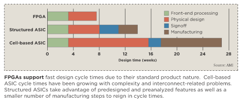
Structured ASICs offer advantages in cost and reduced design cycle time compared with traditional cell-based ASICs. For most applications, the cell-based development costs are just too high due to expensive reticles and design tools plus increased design time. Design time has risen primarily due to interconnect-related problems. Interconnect delays are not scaling down with technology generations the same way transistor delays are. Wire delays are less predictable, and there are crosstalk and power supply voltage drop issues to contend with.
The content of digital ASIC devices is also changing significantly. Chip area tends to be dominated by I/O functions, memories and other large intellectual-property (IP) blocks where performance or density is needed. Logic gate counts are rising, but logic is taking up a smaller percentage of the total silicon die area.
Structured ASICs reduce the reticle costs and design effort. Unlike cell-based ASICs that customize the full reticle set, structured ASICs customize only a small number of metal and via levels.
Design cycle time savings result from using predesigned structures wherever possible, such as I/O rings, power grids and the floor plan where IP blocks, such as memories and timing generators, will be located. Power buses are carefully analyzed ahead of time and are overdesigned for worst-case design scenarios. Some extra area is expended, but as long as the design remains pad-limited, it's not an issue. Some structured ASICs employ pre-routed clock signals. AMIS elected not to preroute clocks because there can be a significant dynamic-power penalty and loss of flexibility in clock tree design.
For structured-ASIC architectures, most of the design effort focuses on place and route and achieving timing closure. The hybrid structured ASIC with its relatively fast and more predictable interconnect simplifies the timing-closure problem compared to the effort required for UDSM copper interconnect.
The lower NRE cost and fast cycle times of structured ASICs are even more valuable if a design ECO or silicon spin is required. In this case, the total project cost and span can be many times shorter than a competing cell-based ASIC solution.
Many applications in the communications, computing, medical and industrial markets do not need the bleeding-edge performance of the most advanced UDSM technologies, especially if the design starts as an FPGA prototype and is then converted to an ASIC for volume production. The hybrid-process structured ASIC fills the gap between FPGAs and UDSM cell-based ASICs with useful native operating voltages, good performance, low power, sufficient density to remain pad-limited, low NRE and short design cycle times.
Bob Kirk is director of system architecture and applications engineering for structured digital products at AMI Semiconductor (Pocatello, Idaho).
Copyright © 2003 CMP Media, LLC
![]()
|
|
|
|
|
|