![]()
|
|
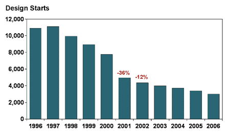
The past few years have seen substantial shifts in how logic content is delivered into electronic systems. The most dramatic of these changes is the sharp reduction of traditional ASIC design starts - according to Gartner/Dataquest, there are about 1/3rd the number of ASIC designs today compared to 3 or more years ago (see Figure 1, below).
ASIC designs have been impacted by the global economic downturn, to be sure, but the sharpness of the drop in design starts is likely due to traditional ASICs becoming far too expensive for most applications. Skyrocketing mask costs, high tool costs and high development costs have ensured that only very high-volume designs can be supported with cell-based ASICs. For mid-volume ASIC designs, the costs are simply becoming out of reach.
In some cases, what previously would have been done as an ASIC is now done as one or more FPGAs, despite their high unit costs, limited performance, and high power consumption and power dissipation. With uncertainty of demand for many products, this has given system manufacturers the ability to get a product in the market and then perhaps pursue cost-reduction if the market takes off.
This is good in theory, but in practice few companies have the incentive to spend design resources and millions of dollars in NRE to convert to a traditional ASIC. In practice, those resources are put into the next product, while the current product continues to ship with hundreds (sometimes thousands) of dollars worth of FPGA content per unit. Potential savings of millions of dollars in manufacturing can't be realized, because the ASIC development costs are in the millions also.
In other cases ASIC designs are not a part of system development anymore because the logic content can be implemented using ASSPs (Application Specific Standard Products), with software used to differentiate the product and add needed functions not provided for in the ASSP. For commodity products in particular, this offers many advantages in both cost and time-to-market.
However, almost by definition, this is not an approach that applies for many high performance or leading-edge products, because these products rely on functions being implemented in hardware for performance reasons, or by implementing functions that have never been done before. Off-the-shelf components cannot meet these needs that typically require a traditional ASIC to be used - but the steep cost of traditional ASIC is now making it economically difficult to not make product compromises in order to use an ASSP.
Emergence of structured ASICs
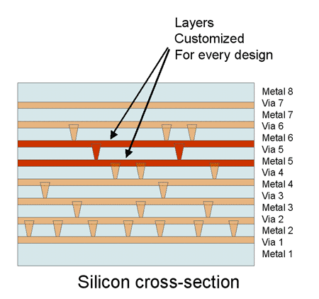
Structured ASICs represent a new ASIC capability that offer a promising alternative to cell-based ASICs for the large mid-volume market. Similar to gate arrays of the past, structured ASICs use pre-diffused base metal layers to implement functions that would be common to many designs - I/Os, memories, power grids, clock networks, and in some cases intellectual property (IP). The custom logic is then implemented in a few metal layers, typically between two to five metal layers, thus requiring far fewer mask layers be created for each design (see Figure 2).
The result is that the NRE charges can be brought down to $100K or $200K, instead of more than a million dollars due to the greatly reduced mask, fab processing, and ASIC vendor engineering costs. In addition, just like gate arrays of the past, these structured ASICs can be delivered to the customer more quickly, thus making them attractive for prototyping and system development.
To be clear, these are not gate arrays. While there is the similarity of pre-diffused silicon layers, in almost all other respects structured ASICs are very different. At the root of these differences is the fact that gate arrays were all about reducing manufacturing cycle time. In contrast, structured ASICs are all about reducing design cycle time, design cost, and design resources.
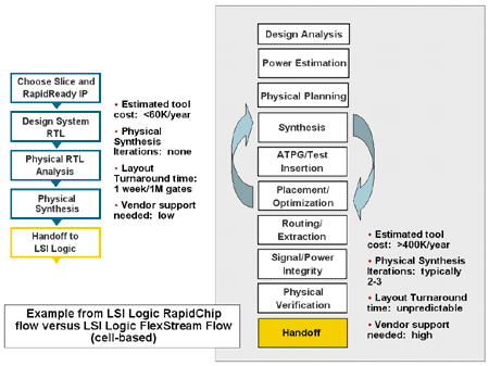
The ASIC vendors in this market have all architected their structured ASIC products to eliminate design flow steps, such as test development and insertion, power grid design and analysis, and signal integrity analysis. Difficult or tedious tasks such as IP integration and memory insertion have also been "designed out" for the user in the structured ASIC devices. In addition to reducing the number of tools needed, structured ASIC vendors have greatly reduced the design cycle time and number of engineers needed in the design team (see Figure 3).
Opportunity for new (and improved) design flow
In taking control of the design flow and methodology for these devices, structured ASIC vendors have worked on all aspects of the overall design process. This includes making sure the design tools used are seamlessly integrated with the vendor's methodology. It also has lead to a basic question: should "one-size-fits-all" tools be used for designing into highly optimized silicon structures?
Many structured ASIC vendors are answering "no." Because the silicon structures and design methodologies are so closely tied together, using generic tools would carry forward much of the baggage that has made ASIC design increasingly difficult and cumbersome. Would you use a sledgehammer to make a beautiful sculpture when a chisel is more appropriate? Of course not. Then why use generic design tools with thousands of switches and commands, with slow runtimes and large memory footprints, when a major point of combining silicon and design automation is to streamline the process and gain substantial time to market advantages? Just like with the sculpture, a customized design tool makes more sense.
The other major advantage customized design tools offer is that the performance realized in the silicon can be substantially faster. By customizing the synthesis tool for a specific structured ASIC architecture, typical performance improvements of 15 or 20% can be seen versus using generic tools - on both timing and area, simultaneously.
This means that the decreased performance and density inherent in a structured ASIC can be mostly (if not fully) recovered by using tools the ASIC vendor has jointly engineered with the EDA vendor. Effectively, this means performance and density have been taken off the table with respect to whether a system design might use a cell-based ASIC or a structured ASIC to meet their system goals. This is a revolutionary aspect of structured ASIC technology.
To see how this performance improvement is achieved we can look at a few examples. The NEC ISSP (Instant Silicon Solution Platform) structured ASIC technology is a mux-based fabric. With a mux-based architecture, typically there are asymmetrical delays across a cell in the design library; this can result in up to a 25% difference in timing for paths through the cell (see Figure 4).
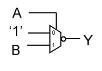
Generic synthesis tools, in the spirit of one-size-fits-all, treat paths through the cell as being symmetrical, and thus will incorrectly calculate the true circuit timing. Similarly, no generic synthesis tool will keep track of (or optimize) for the specific ratio of flops, inverters, and muxes that the ISSP fabric is comprised of.
This means that the generic synthesis tool will almost always overuse some of these elements and under-use others; there is no balancing of the design resources to maximize logic density. Customized synthesis tools that can perform automatic resource balancing, particularly in developing arithmetic and datapath operators, can achieve simultaneously better area and timing performance.
Many other customizations to the synthesis process can be done to extract higher performance and density. These include synthesizing directly to large cells in the library, instead of base primitive cells. This leads to more efficient use of base cells in general (better resource balancing), and can lead to easier place and route through fewer pin-pairs needing to be routed. Customizing synthesis allows practically all synthesis optimization "tricks" to be specifically tuned to the base architecture, so that decisions are made knowing more precisely how the structures will be implemented.
Physical synthesis
These same concepts can be extended into physical synthesis, where it becomes even more important to be vendor-specific in the tools used prior to final routing and layout by the ASIC vendor. By working closely together, the EDA vendor and structured ASIC vendor can build into the physical synthesis tool such elements as:
One example of this is how structured ASIC devices have a power grid already developed and pre-diffused in the base layers. With a cell based ASIC design the physical synthesis tool is only working off of "guesstimates" provided by the designer in their floorplan, not on the actual power grid itself. Not surprisingly, when the actual power routing is done by the cell-based ASIC vendor, many factors will change such as the space required by the power routes, the IR drop effect of the power grid, and how critical cells are placed with respect to the power grid. This leads to the design closure problem.
In contrast, a structured ASIC with a predefined power grid allows the physical synthesis flow to actively use the power grid directly in physical synthesis. With a power grid, instantaneous IR drop calculations can be performed directly in physical synthesis; that way the tool can understand the true voltage received by each cell, and therefore make a more accurate assessment of timing across that cell (see Figure 5).
Likewise, placement of cells with respect to the power grid and other high activity cells in the design can be done automatically by the physical synthesis tool, instead of it being an after-the-fact and possibly iterative operation by the ASIC vendor. Furthermore, with this more detailed knowledge of the routing structures the physical synthesis tool can automatically perform vendor-specific design rules checking on a more complete design, further ensuring that when the placement and netlist are handed off to the structured ASIC vendor that the design is only handed off once without iterations.
The goal of most ASIC design teams is to minimize risk, both to the chip design project and to the system integration. Structured ASIC devices offer complex ASIC technology with 75%, or less, the development cost of a cell-based ASIC, while being up to 90% less than the cost of a complex FPGA. Structured ASIC technology offers user differentiation, in hardware, more quickly than custom software development might be for an ASSP. Perhaps most importantly, they offer customized and tested design methodologies that reduce design risk, cost, and complexity, while maximizing the performance, density, and time-to-market attributes of structured ASICs.
The number of announced ASIC vendors offering structured ASIC devices continues to grow, with 8 vendors having officially announced products in this space, including NEC, LSI Logic, Fujitsu, Lightspeed, and others. The commitment from these ASIC vendors to offer design flows that offer substantial improvements in lower risk, lower cost, higher automation, and higher performance is clear.
John Gallagher is director of marketing for Synplicity's ASIC synthesis technologies. Prior to joining Synplicity in 1999, he served as director of place and route marketing at Cadence Design Systems. He has also held ASIC marketing positions at LSI Logic and Hewlett Packard.
Copyright © 2003 CMP Media, LLC | Privacy Statement
![]()
|
|
|
|
|
|