![]()
|
|
|
|
 |

ASIC spin-offs seek success amid established alternatives
by Brian Dipert, Technical Editor
You have a diverse set of silicon resources to choose from, and vendors are tailoring their building-block portfolios to meet your needs.
So, you've decided that buying and hooking together off-the-shelf ASSPs (application-specific standard products), such as embedded controllers, peripheral chips, and the like, and then writing your own software, will fail to provide your design sufficient differentiation from competitors' products. As a result, you elect to tackle chip-level design. The two leading silicon-platform contenders and their respective trade-offs have by this time been extensively debated in a variety of industry forums, but if you're new to the game, here's a summary.
FPGAs are becoming increasingly dense in gate count on a per-chip basis, thanks to the deep-submicron processes on which they're manufactured, such as Xilinx's 90nm process for its latest Spartan-3 family (Reference 1). The usable capacity they deliver is particularly lofty if your design employs their embedded memory arrays and diffused analog-and digital-function blocks, such as DLLs and PLLs, multiply-accumulators, SERDES (serializer/ deserializer) circuits, high-speed I/O buffers, and, in some cases, even CPU cores and associated peripherals. You can order as few or as many FPGAs as your design requires, and you need not pay NRE (nonrecurring-engineering) charges to their supplier. The vendor has already laid out and debugged the chips' logic, memory, signal-routing, and power planes.
Once your design is complete, you can have a working chip in your hands within seconds to minutes. And, generally speaking, the tools you use to develop and debug your designs are much less expensive than those for their ASIC counterparts. (However, if Hier Design's $25,000 PlanAhead indicates future industry trends, the average prices of FPGA tool sets are rising.) No matter how dense FPGAs become, though, they remain one to two orders of magnitude less efficient in area than standard-cell ASICs built on a comparable process. FPGAs, especially those based on a silicon-gobbling, six-transistor-per-cell SRAM LUT (look-up-table) and configuration-element technology, are also significantly more power-hungry than their ASIC counterparts.
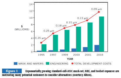
ASICs' advantages unfortunately come with a corresponding set of shortcomings. NRE charges, minimum-order quantities, and per-seat development-tool-suite costs are skyrocketing as the chips migrate down the Moore's Law lithography path (Figure 1). An ASIC's minimum-order quantity is a reflection of the fewest possible customer-specific wafers the vendor can run down the manufacturing line and still turn a profit. The larger the chip's die, the smaller the minimum required order quantity, and you can also see why transitions to smaller process lithographies and larger wafers have dramatically increased this minimum-volume requirement.
The time you need to track down and fix exotic bugs caused by power-supply droop, signal coupling, and other deep-sub-micron-routing effects combines with routing-dominated timing closure exertions to distend standard-cell-ASIC-development cycles. Even when you think your design is complete, you still have to wait for it to go through lengthy fabrication, test, and packaging steps before you get chips back, and, if they don't work or if they no longer meet quickly changing market needs, you incur multipli-cative costs and delays. Designing with standard-cell ASICs requires a lot of time, work, and money; these factors are some of the reasons for the dramatic market shift toward FPGAs, as recent analyst reports document. But for design gate counts or chip volumes in hundreds of thousands or for performance-critical or power-stringent designs, standard-cell ASICs remain the only game in town.
Conventional solutions
Or are they? To answer this question, first compare FPGAs' and ASICs' fundamental silicon building blocks: their logic cells and routing structures. FPGAs' logic cells are coarse-grained, ranging from collections of multiplexers and discrete-logic gates to one or several LUTs and usually supplemented by flip-flops. Actel's ProASIC FPGAs currently offer the finest grained logic blocks in the industry. FPGA vendors design their devices' intralogic-block routing, thus minimizing the number of required user-configurable routing layers; the design compilation and placement-and-routing software thus faces the primary challenge of making efficient use of the logic blocks. The chips come to you with mostly unprogrammed interlogic-block routing resources; you configure them either before system power-up for antifuse- and flash-based chips or at and, if your design supports it, after power-up for SRAM-based FPGAs.
Standard-cell ASICs' logic blocks are much finer grained than those FPGAs. As the "standard-cell" designation implies, they employ consistently sized dimensions for transistors and other on-chip structures. (This homogeny is their key differentiation from a full custom chip.) However, as the designation "application-specific" implies, their placement along with the device's clock, power, and signal routing are specific to your implementation. As a result, all of the chips' metal and polysilicon layers are unique for each customer, and the vendor pre-configures the routing before shipping the device to you, leaving you with no hardware-customization capability during system manufacturing and subsequent operation. The development software in this case focuses not so much on making the design implementation within each logic block efficient, as is the case with coarser-grained FPGAs, but in efficiently interconnecting the blocks.
Historically, another ASIC category, the gate array, sat between the FPGA and standard-cell-ASIC extremes. Like an FPGA, a gate array's routing mesh was generic and predetermined. Like a standard cell, the design-specific configuration of this routing mesh occurred during the final few stages of chip manufacturing, and vendors sometimes referred to the fine-grained logic-cell array as a "sea of two-input NAND gates." Gate arrays have faded from widespread usage in recent years, victims of the jack-of-all-trades, master-of-none phenomenon that became increasingly evident as FPGAs encroached on their turf. Their order-to-availability turn-around time wasn't sufficiently faster than a standard cells' to capture a large chunk of FPGA business. And their performance and silicon efficiency were too poor to enable them to take over many standard-cell opportunities.
Mask-programmable FPGAs
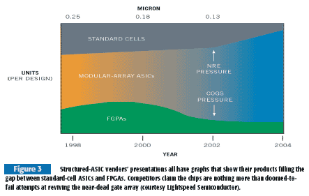
Some ASIC suppliers, alarmed by the evaporation of their business, have combined a page or two from the FPGA book of tricks with lessons learned in their gate-array past lives to come up with the structured ASIC. Some also refer to this approach as a modular array or structured array. Plenty of vendor-to-vendor technological differences exist, but simplistically speaking, a structured ASIC is a gate-array derivative with an FPGA-like, coarse-grained logic cell, thereby requiring fewer user-configurable metal and via layers (Figure 2). The vendor handles clock-tree and power-plane routing. An analogy might prove helpful in under-standing the structured-ASIC pitch: In the early days of software programming, microprocessors were slow, and memory was expensive, so low-level, highly efficient assembly language and even lower level machine code dominated.

As CPUs have grown faster and memory has become cheaper, higher level software languages have taken over. They use resources less efficiently, but efficiency isn't so essential nowadays. Time to market is increasingly important, though, and high-level languages excel in this regard. For similar reasons, VHDL and Verilog are increasingly the design-entry methods that hardware engineers who put circuits into chips choose over the more time-consuming schematic-capture technique. The structured-ASIC vendors are gambling that a market will also emerge for a silicon platform that, although it may be less efficient than a standard cell and deliver a longer time to market than an FPGA, doesn't exhibit the full extent of those competitors' shortcomings, either (Figure 3).
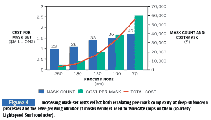
Because a high percentage of the chips' masks-conveniently, often also the most expensive masks-are generic to multiple customers' designs, the per-customer NRE charges and turnaround times decrease, and you can also more easily adapt the resulting platform to evolving industry standards and to spinoff chips containing minimally altered hardware (Figure 4).
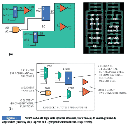
AMI Semiconductor, Chip Express, Faraday Technology, Fujitsu, Lightspeed Semiconductor, NEC, and ViASIC are some of the companies now touting their structured-ASIC wares. AMI is the only vendor on this list not currently positioning itself as a broad-based silicon supplier; the company is sticking with its FPGA conversion niche but employing a structured-ASIC foundation instead of the gate-array platform of the past. Conversely, Lightspeed Semi-conductor has retreated from a brief expansion into the Xilinx FPGA cost-reduction market to exclusively focus on conventional ASICs (Reference 2). Chip Express's structured ASICs employ perhaps the finest-grained logic block of the various alternatives; the vendor estimates that its devices will encompass three to four gates per logic module, depending on the design. Most of the other vendors' logic blocks each implement 20 to 40 gates' worth of your design (Figure 5).
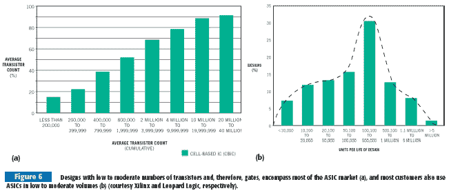
Structured-ASIC suppliers build their chips on a diverse mix of processes. This multiplicity reflects each vendor's attempt to tailor its offerings for an exclusive slice of the potential customer-base pie. Vendors and, where applicable, their foundries have already amortized the fabrication facilities and equipment they use to build trailing-edge, well-understood, and high-yielding, 0.18-, 0.25-, and 0.35-micron processes. There's an upper limit to the design size you can implement in them, but the relevant vendors point out the analyst reports indicating a large percentage of ASIC designs having fewer than 1 million gates, along with data suggesting that customers use half of all ASIC designs in volumes of less than 100,000 units (Figure 6).
On the other end of the spectrum are companies such as Fujitsu, which has a 0.11-micron structured-ASIC process now in production and a 0.09-micron process coming out in 2004, and NEC, which forecasts that its 90nm process will also be in production by the second half of next year. Tailoring the process to the design is a delicate balancing act that also involves comprehending the design's I/O-buffer count; the last thing the vendor and customer want to have happen is for the die to contain unused, thereby silicon-wasting area within a minimum-size-constraining I/O ring. Escalating costs for complex packages also make the cost of any silicon inside the package proportionally irrelevant (Reference 3).
Structured-ASIC suppliers claim to shrink the many-month standard-cell turnaround from design handoff to availability of first samples to a few weeks. This delay isn't quite the few-second to minute lag time from placed-and-routed netlist to silicon that FPGAs deliver, but ASIC advocates assert that this comparison is in some sense a case of apples versus oranges. They point out that, as FPGAs and the designs within them grow in complexity, engineers are spending an exponentially increasing amount of time struggling to achieve area ("will it fit?") and timing ("will it run fast enough?") closure. Because an ASIC is an inherently faster design foundation than an FPGA, they maintain, you'll spend less time in simulation and redesign, and, therefore, your total development cycle may be shorter with a structured ASIC than with an FPGA.
Hardware-customizable ASSPs
One means by which structured-ASIC suppliers maximize the speed of performance-critical circuits, as well as implement other efficiencies, such as area and power improvements, is by putting these circuits into diffused portions of the chip instead of into generic-logic structures. Fujitsu, for example, claims that its diffused embedded flip-flops reduce power dissipation by a factor of two and improve gate usage by 1.5 to two times over alternative approaches. Lightspeed embeds AutoTest and AutoBIST at-speed testing circuits within its Modular Array ASICs to ensure 100% stuck-at fault coverage and to catch deep-submicron-induced delay faults. Every structured ASIC supplier that this article mentions offers diffused embedded-SRAM blocks, and several of them can integrate timing circuits, high-speed serial and parallel I/O buffers, and other analog-rich and area-, power-, and performance-critical structures if your design requires them.
LSI Logic takes diffused circuits to an extreme with its RapidChips, which the vendor refers to as platform ASICs and currently builds on both its 0.11- and 0.18-micron processes. The company hopes that RapidChip will enable it to revisit the happier times of a few years ago, when its customers were handing it an average of three design starts per day; now, it sees a new design roughly every three days. LSI Logic begins with an application-tailored mix of diffused analog, digital, and memory resources that consume a large percentage of the die, such as SRAM arrays, microprocessor cores, PLLs, and SERDES-based interfaces, such as 10Gbit Ethernet, Fibre Channel, and SATA. It supplements these dedicated functions with one array or multiple arrays of on-chip gate-array ASICs and calls the resultant chip a RapidSlice. LSI Logic's Extreme families are application-tailored in their extensive diffused core inclusion; Integrator products are more generic in nature.
Reflecting the fine-grained gate-array logic cell, RapidChip parts support user customization of as many as five layers of metal. The transition from generic RapidSlice to customer-specific RapidChip involves the population of the gate-array partitions, potentially both with customer-designed proprietary circuits and with cores licensed from LSI Logic's CoreWare library. These cores can be "soft,""hard," or "firm" IP (intellectual property). Soft IP has the greatest layout flexibility but the lowest performance; hard IP with predefined placement and routing, which the company calls Hard RapidReady IP to differentiate it from the prebuilt Diffused RapidReady cores, is at the opposite end of the speed-versus-adaptability spectrum. Firm IP is preplaced but not routed and is therefore an interim step between the other variants. LSI Logic claims that a straightforward cost-reducing path exists from RapidChips to its IP-compatible standard-cell ASICs.
The RapidChip program focuses not only on the silicon portion of the implementation equation but also on development-tool expenditures-particularly an issue in this era of lingering high-technology recession. The RapidChip libraries will plug into any expensive standard-cell ASIC tool suite that you already own; other ASIC vendors' libraries also work in this fashion (Reference 4). LSI Logic has also partnered with Synplicity and Tera Systems to deliver RapidWorx, an integrated, comprehensive tool set incorpor-ating physical synthesis, RTL-rule checking, and planning capabilities; it has a $20,000/six-month licensing fee. Synplicity, a long-dominant design-software presence in the FPGA market, is intimately familiar with a business approach that trades off a lower per-design-seat profit margin for a much larger number of design seats. Traditionally ASIC-focused EDA suppliers will find this transition difficult, to say the least, and Synplicity is hoping that this second stab at the ASIC market will prove more successful than its Synplify ASIC product has so far been. Synplicity has also announced relationships with Chip Express, Lightspeed, and NEC.
Competitors scoff at structured-ASIC vendors' claims. Actel and QuickLogic, for example, point out that their antifuse FPGAs offer much greater design and manufacturing flexibility than and density and performance comparable to that of the similarly coarse-grained-structured ASICs. Actel's vice president of marketing, Barry Marsh, also thinks that a cultural factor is at work in the structured-ASIC push: Asian vendors are sometimes forced to take low-volume business they normally wouldn't accept, due to "relationship" factors, and structured ASICs give them a means of supporting this business at a potentially profitable level.
ASIC suppliers without structured-ASIC programs-or at least publicly announced programs-such as IBM and Toshiba, also predictably denigrate the newcomers' abilities to meet their lofty goals. Toshiba believes that, because FPGAs and standard-cell ASICs are both well-established in the industry, the gap between the two in cost, performance, power consumption, time to market, or any other factor is too small for any of the structured-ASIC suppliers to long survive. Toshiba reports that in recent years it has made significant investments in its IP library, verification method-ology, and back-end tools; its goal is to reduce its handoff-to-production delay to less than six months.
Toshiba claims that routing errors, not logic bugs, necessitate most design respins and, therefore, a hybrid standard-cell-plus-gate-array platform, such as the one that it offers, will meet most customers' needs. Xilinx has similar pessimistic feedback about structured-ASIC vendors' prospects; the company believes that, by migrating its FPGAs to advanced lithographies, it can negate any advantages that the comparably trailing-edge-process-based structured-ASIC might otherwise possess (Figure 7).

Varied responses Xilinx also points out that LSI Logic's RapidChip looks suspiciously similar in concept to its own Virtex-II Pro platform, containing diffused PowerPC cores and other circuits and swapping out RapidChip's mask-programmable partitions for more flexible SRAM-based programmable logic. Other FPGA-inclusive examples of hybrid chips include Altera's Excalibur line, Atmel's FPSLIC (field-programmable system-level IC) chips, Quick-Logic's Embedded Standard Products, and Triscend's Configur-able Systems on Chips (references 5 and 6). IBM's partnership with Xilinx gives Big Blue access to its partner's FPGA technology; although IBM has not yet announced any tangible results of the relationship, industry pundits believe that the company plans to soon roll out the ability to embed FPGA cores within its standard-cell ASICs.
Altera's evolving position on ASICs has been interesting to observe and analyze. Until a few months ago, the company, like its key competitor, Xilinx, was a vociferous critic of ASIC technology. However, Altera recently introduced the latest iteration of its HardCopy FPGA-conversion platform, targeting latest generation Stratix FPGAs. The companion $2000/year Quartus II Version 3 design software now supports the notable ability to directly compile your design to HardCopy, thereby bypassing the interim Stratix step and in effect transforming Altera into a structured-ASIC supplier. Altera's vice president of marketing, Tim Colleran, says the company will likely entertain potential HardCopy business with volumes of 5000 units or more per year and will base any variation on that figure on the customer and the device. NRE charges will be approximately $200,000 and are similarly adaptable to customers, devices, and volumes. Altera can turn around HardCopy samples to you in approximately eight weeks and production units in roughly 18 weeks. Until you receive production HardCopy chips, you can use FPGAs; keep in mind, though, that HardCopy devices in some cases have less on-chip memory than their FPGA counterparts, and they also come in fewer, cost-optimized packaging options.
Altera estimates that HardCopy chips are, on average, 50% faster, 70% smaller, and use 40% less power than their FPGA counterparts. This broadening of Altera's product capabilities may reflect the influence of Altera's new chief executive officer, John Daane, formerly a vice president at LSI Logic. Xilinx dismisses HardCopy's importance and offers EasyPath, its own cost-reduction program. Not too long ago, though, Xilinx had HardWire, a HardCopy-like product line of its own, and the company also doesn't divulge the ideas it's brewing in its R&D labs. The silicon foundation for EasyPath is the same FPGA that you'd normally buy, but Xilinx tests it with a customer-specific flow that typically results in higher yields. The altered flow no longer screens for potentially nonfunctional portions of the chip that your design doesn't use, and it loosens normally stringent ac and dc specifications as appropriate for your design's needs.
FPGA start-up Leopard Logic also believes a future exists for ASIC-plus-programmable-logic hybrids. The company emerged a few years ago as a promoter of embedded-FPGA technology to ASIC vendors and foundries and their end customers. Like Actel, Adaptive Silicon, and other companies that preceded it down the embedded FPGA path, Leopard Logic has garnered little success with its pitch; company officials attribute the primary blame to risk-averse venture capitalists that caused a cash crunch when they stopped investing in IP companies. Leopard Logic is reinventing itself as a fabless-ASIC supplier, incorporating its embedded-FPGA technology and targeting year-end for an initial product launch.
References
Author Information
Technical editor Brian Dipert is confident that, with all these silicon-building-block options arm-wrestling in the market, he'll have plenty to write about in the future. Reach him at 1-916-454-5242, fax 1-617-558-4470, bdipert@edn.com, and www.bdipert.com.
At a glance
For more information on products such as those discussed in this article, go to www.edna-enq.com and enter the reader sevice number. When you contact any of the following manufacturers directly, please let them know you read about their products in EDN Asia.
EDN Asia's SUPER INFO NUMBER
For more information from all the vendors listed in this box, you need enter only one number.
Enter No.483
<!-- saved from url=(0038)http://www.ednasia.com/jan04/df2.html -->
![]()
|
|
|
|