![]()
|
|
|
|
| Source: http://www.fsa.org/pubs/fablessforum/article.asp?article=0306/tamme |
|
|
|||
|
[ FABLESS FORUM ] To FP or GA - That's the Question Stefan Tamme, Vice President of Sales & Marketing, Leopard Logic, Inc. Boom or bust, some things don't seem to change. It's still all about time and money, as companies have to decide how to implement their next design and what implementation platform to choose. Rapidly increasing mask costs and lengthening design cycles of application-specific ICs (ASICs) necessitate new solutions to produce custom logic devices on time and on budget. This dilemma is driving the field programmable gate array (FPGA) market today and has caused the recent resurgence of gate-array style devices. As fewer companies can afford cell-based ASIC designs, they revert to less-costly solutions or try to replace custom logic devices with off-the-shelf application-specific standard products (ASSPs). FPGAs offer a great alternative, as they combine the economies of scale of a standard product with the customizability of an ASIC. However, this flexibility comes at a high price in terms of higher unit costs, higher power consumption and lower capacity and performance. Embedded FPGA technology kills two birds with one stone, as it enables the combination of the flexibility and time-to-market of FPGAs with the capacity and performance of an ASIC in a new class of hybrid devices. This market is forecast to skyrocket to over $650 million in 2007 at a CAGR of 115%, according to market research firm In-Stat/MDR. The Alternatives and Tradeoffs System companies demand flexible chip-level solutions that allow them to add value and differentiate their products. Shrinking product life cycles combined with rising performance and capacity requirements mandate the use of innovative IC technologies to meet today’s market demands. Traditional design approaches including ASICs, FPGAs and ASSPs all address some of the needs, but have significant shortcomings in other areas:
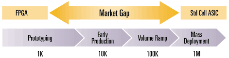
Lately, there have also been attempts to use reconfigurable processor arrays to replace logic devices. However, the key issue with these architectures is the fundamentally different design methodology and programming model. Users are required to start their development from scratch and cannot re-use existing intellectual property (IP) blocks or design tools. The design flows are complex and require long learning curves to produce efficient results. Market Trends Advanced 90-nanometer process technology will make things worse - or better, depending on the perspective. While mask charges will continue to increase, and design and tooling costs spindle out of control, every process node will make FPGA-based products more attractive. Silicon cost is no longer the main cost factor for the majority of products, as amortized NRE, packaging and test become the dominant cost drivers. Looking back in history, disk storage limited the amount of data stored on a computer and mandated software efficiency. Then, the emergence of low-cost storage enabled new approaches to programming, as software developers moved to library and component-based methodologies. The equivalent trend is happening in chip design today, as larger designs are assembled from existing components (i.e., silicon IP blocks). As the industry continues to drive device costs down, the current focus on die area will become less critical as more focus is put on flexible implementations and short development cycles. Once believed the panacea to lowering their component costs, most OEMs are now abandoning their internal customerowned tooling (COT) flows and are reverting back to an ASIC style design flow, using outsourcing and traditional ASIC vendors. Whenever designs require extreme performance, capacity or lowest power, standard cell ASICs will likely remain the technology of choice, as long as the volume and price points justify the business case. On the other end of the spectrum, FPGAs have a bright future for low-volume applications and in high-volume, but lowcomplexity, applications. For a growing number of designs however, neither of these options seems to work. Latest statistics show that about 80% of ASICs never exceed 500K lifetime units. The median design complexity currently is about 1.2M gates (800K logic and 400K memory). Despite the marketing claims of FPGA vendors, even the largest FPGAs still have to crack the 1M logic gate mark. The result is a growing number of ASIC users seeking viable alternatives. The result of these trends is that there is a growing number of designs that cannot be addressed effectively with either ASIC or FPGA. Figure 1 illustrates this market gap between FPGAs and standard cell ASICs in the volume range between 1,000 units to 100,000 units per year. Figure 1. Market Gap Between FPGAs and ASICs
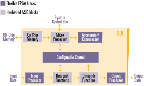
The Renaissance of the Gate Array? There are numerous efforts underway to address this fastgrowing opportunity in the mid-range logic market. Besides some more esoteric approaches like configurable processor arrays, there seems to be a resurgence of gate arrays in various forms. Vendors are careful not to use the term "gate array," as analysts have put those devices on the endangered species list. But when looking under the hood, these approaches certainly fall into this category. While there is nothing wrong with this, most of these newage gate arrays do not address some of the fundamental issues of flexibility and short time to revenue. They still use the traditional ASIC model where the designer submits the netlist or RTL to the device vendor, waits for several weeks and then hopes that timing closure has magically happened. If not, the process repeats itself until the design finally meets timing closure and can be released to production. Most vendors use two to four layers of metal for the customization, which helps with mask costs and turnaround times, but still requires significant mask costs of over $100,000 and typically six to eight weeks turnaround time. The Future is Hybrid The recent emergence of embedded programmable logic cores enables the creation of flexible, yet cost-effective hybrid device platforms. Such platforms are ideally suited for a variety of applications such as digital signal processor (DSP) and packet processing and allow for fast timeto- volume at attractive price points. Embedded FPGA will follow in the footsteps of embedded memory and embedded processors to become one of the fundamental building blocks of future system-on-chip (SOC) devices. Design functions that are fixed or low-risk, such as larger data path functions, are implemented in an ASIC fabric, while high-risk blocks and functions that require field-upgradeability are placed into the FPGA cores. This partitioning provides FPGA-like design cycles and flexibility, while achieving ASIC-like performance, power and cost. Figure 2 shows a generic SOC block diagram that identifies some of the key areas requiring design flexibility to mitigate risk, enable fast derivatives and provide protection against evolving standard and interoperability requirements. Figure 2. Partitioning Between Hardwired and Flexible Functions
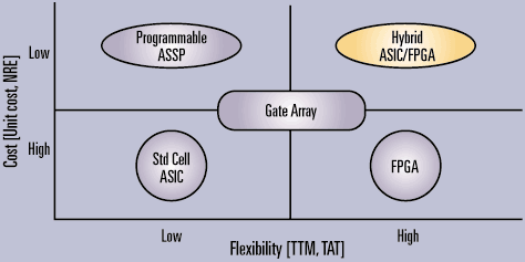
As many chip markets continue to fragment, hybrid devices will offer a new alternative for designers to partition their design. In the past, designers were forced to partition their design into multiple devices to achieve the right trade-off between flexibility, performance cost and power. This partitioning had to happen early in the design process to account for long ASIC design cycles. With this approach, the system partitioning was usually sub-optimal and could not be changed at a later time. Figure 3 compares the different approaches with respect to cost and flexibility. Costs are measured as total cost of ownership (TOC), taking into account unit cost and fully loaded NRE. Flexibility is measured as time-to-market (TTM) and turnaround time (TAT) required for incremental design changes. Figure 3. Flexibility/Cost Comparison
Hybrid ASIC/FPGA solutions enable the most effective trade-offs, as they allow users to tap on a wealth of existing IP blocks, methodologies and design tools. With the right partitioning, these devices allow instant design changes like FPGAs, while leveraging the more efficient ASIC logic for fixed blocks of a design. These characteristics make hybrid devices the ideal next evolutionary step for products that otherwise fall into the market gap. When the electronic equipment markets recover, there will be a rush to get new products designed quickly and deployed cost-effectively, providing a tremendous opportunity for hybrid devices. About the Author Stefan Tamme is vice president of sales & marketing at Leopard Logic, Inc. and has over 15 years of marketing, sales and engineering experience in semiconductors, systems and software. Prior to Leopard Logic, he served in the same role at AXYS Design Automation. Formerly, he ran the U.S. operations and international business development for Sican (now sci-worx). He began his career developing sensor systems and later joined Bosch as a software developer. stefan@leopardlogic.com; 650-400-5151 |
|||
|
|
|||
|
©1994-2003 Fabless Semiconductor Association |
|||
|
|
|
|