|
|
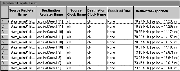
Reports the maximum frequency (fMAX) of the 10 slowest register-to-register paths. In addition, the section lists any frequency requirements specified for the listed source and/or destination registers. The Register-to-Register Fmax section reports essentially the same data as the fmax section (Compilation Report), except the data is organized differently. The register-to-register timing information is displayed in a resizable, multicolumn table. If you specify any timing requirements for the listed source and/or destination registers, and the timing requirements are not achieved, the information in the table rows appears in red.
| You can change the number of paths displayed by specifying timing analysis reporting restrictions. You can eliminate unwanted source and destination paths from the timing analysis by specifying project-wide timing requirements and/or assigning the Cut Timing Path timing assignment to an individual node by following the steps for making individual timing assignments. |
The following figure shows an excerpt from the Register-to-Register Fmax section of a sample design:
You can select a source or destination register in the Register-to-Register Fmax section and choose List Paths (right button pop-up menu) to display the delay paths associated with the selected register-to-register path. When you choose List Paths, the Messages window displays the time increments that comprise the delay path for the selected register. You can locate the source of the delay path in the Last Compilation floorplan by double-clicking the delay path message in the Messages window. The delay path information is displayed using the following syntax:
Internalfmaxforclock<clock name>betweenregister<source register name>andregister<destination register name>is<fmax value>MHz(Period:<clock period>ns)+Longestregistertoregisterdelayis<delay value>ns1:+IC(<interconnect delay>)+CELL(<cell delay>)=<cumulative delay>;Loc.=<location>; <node type>=<node name>-SmallestClockskewis<clock skew value>ns+ShortestClockpathfrom<clock name>todestinationregisteris<delay value>ns1:+IC(<interconnect delay>)+CELL(<cell delay>)=<cumulative delay>;Loc.=<location>; <node type>=<node name>-LongestClockpathfrom<clock name>tosourceregisteris<delay value>ns1:+IC(<interconnect delay>)+CELL(<cell delay>)=<cumulative delay>;Loc.=<location>; <node type>=<node name>+Microclocktooutputdelayofsourceregisteris<delay value>ns+Microsetupdelayofdestinationregisteris<delay value>ns
The Timing Analyzer calculates the register-to-register performance using the following equations:
<register to register delay> - <clock skew delay> + <micro clock to output delay> + <micro setup delay>
Clock skew delay is calculated with the following equation:
<clock to destination register delay> - <clock to source register delay>
|
- PLDWorld - |
|
|
| Created by chm2web html help conversion utility. |